Phase-change memory write/erase circuit with initializing function and rapid write/erase method thereof

A technology of phase change memory and initialization method, which is applied in the field of write and erase circuits of phase change memory, can solve problems such as the limit of write and erase speed, achieve the effects of improving bit pass rate, realizing high-speed write and erase operations, and uniform resistance distribution

Active Publication Date: 2015-06-17
SHANGHAI INST OF MICROSYSTEM & INFORMATION TECH CHINESE ACAD OF SCI
View PDF4 Cites 2 Cited by
  • Summary
  • Abstract
  • Description
  • Claims
  • Application Information

AI Technical Summary

Problems solved by technology

In this way, the writing and erasing speed of the phase change memory is limited by the speed of the set

Method used


Image

  • Phase-change memory write/erase circuit with initializing function and rapid write/erase method thereof
  • Phase-change memory write/erase circuit with initializing function and rapid write/erase method thereof
  • Phase-change memory write/erase circuit with initializing function and rapid write/erase method thereof

Examples


Embodiment 1

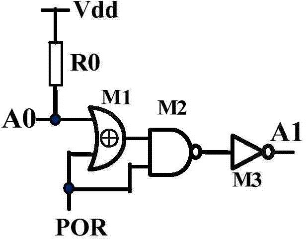
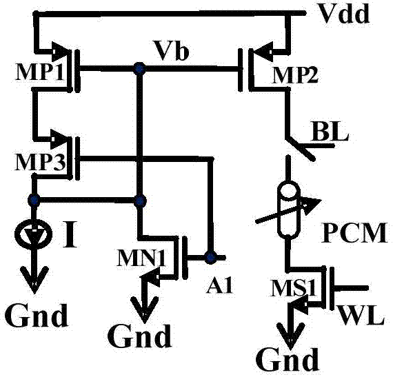
[0037] see Figure 1 to Figure 4, the present invention provides a phase change memory write and erase circuit with initialization function, the phase change memory write and erase circuit at least includes:

[0038] The initialization control circuit is connected to the power supply, and is used to access the power-on reset signal of the internal circuit and the external signal and send out the initialization reset signal;

[0039] The initialization circuit includes an original current source; the initialization circuit is connected to the power supply and the initialization control circuit, and sends a reset current pulse under the control of the initialization reset signal to initialize the phase change memory unit;

[0040] The write-erase control circuit includes a write-erase control signal generation circuit and a write-erase operation circuit connected to the write-erase control signal generation circuit; the write-erase operation circuit is connected between the powe...

Embodiment 2

[0056] The present invention also provides an initialization method of a phase change memory write-erase circuit with an initialization function: when the initialization control circuit receives an internal circuit power-on reset signal and the external signal is in a specified state, the initialization control circuit outputs High level and acts on the initialization circuit; the initialization circuit shields the original current source, so that the power supply directly acts on the phase-change memory unit, so that the phase-change memory unit is reset and initialized; the specified state is low.

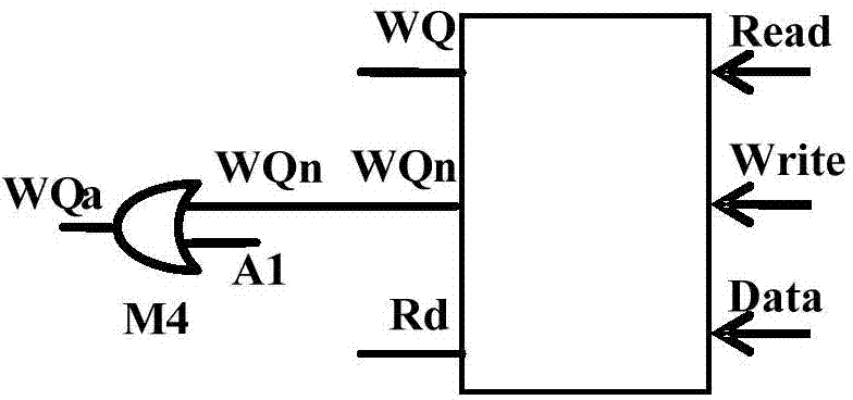
[0057] Specifically, when the silicon wafer (Wafer) is manufactured and stored, and the silicon wafer is tested, the working point of the internal circuit of the chip is established, and a POR signal is sent to allow the initialization of the phase change memory. Such as figure 1 As shown, the external initialization signal is applied to the first input terminal of the XOR gate ...

Embodiment 3

[0064] The present invention also provides a fast writing and erasing method of a phase change memory write and erase circuit with an initialization function: when the phase change memory is working in a normal state after initialization, the write operation adopts a right-angled trapezoidal pulse current that rises rapidly and falls slowly , the pulse height is 0.5-3 mA, the high-level pulse width is 200-400 nanoseconds; the wiping operation uses a rectangular pulse current that rises and falls rapidly, the pulse height is 0.5-3 mA, and the pulse width is 200-400 nanoseconds.

[0065] see Figure 5 and Figure 6 ,in, Figure 5 It shows the current pulse waveform when the phase change memory write-erase circuit with initialization function of the present invention performs an erase operation (Reset); Figure 6 Shown is the current pulse waveform when the phase-change memory write-erase circuit with initialization function of the present invention performs a write operation (...


PUM


Abstract

The invention provides a phase-change memory write / erase circuit with an initializing function. The phase-change memory write / erase circuit at least comprises an initialization control circuit, which is connected to a power supply and is used to receive an electric reset signal of an internal circuit and send an initialization reset signal; an initialization circuit, which comprises an original current source; wherein the initialization circuit is connected to the power supply and the initialization control circuit and sends reset current pulses to initialize the phase-change unit under the control of the initialization reset signal; and a write / erase control circuit, which comprises a write / erase control signal generating circuit and a write / erase operation circuit connected to the write / erase control signal generating circuit, wherein the write / erase operation circuit is arranged between the power supply and the phase-change memory unit. The provided circuit and method can increase the qualified rate of phase-change memory, and enables the phase-change memory to have a rapid write / erase function.

Description

technical field [0001] The invention belongs to the field of semiconductor integrated circuits, and relates to a phase-change memory write-erase circuit with an initialization function and a fast write-erase method thereof. Background technique [0002] Phase-change memory utilizes the crystalline and amorphous properties of phase-change materials to store data. Such phase change materials, such as Ge-Sb-Tb (GST), are amorphous semiconductors of chalcogenides. The phase change unit uses current heating to convert the phase change material from an amorphous state to a crystalline state, that is, the phase change material changes from a high-resistance state to a low-resistance state. This operation is called: set; or phase change The change material changes from a crystalline state to an amorphous state, that is, a phase change material changes from a low-resistance state to a high-resistance state. This operation is called: reset (reset). The two states of crystalline stat...

Claims


Application Information

Patent Timeline
Patent Type & Authority Applications(China)
IPC IPC(8): G11C11/56
CPCG11C13/0004G11C13/0069G11C13/0097
Inventor 陈后鹏李喜王倩范茜胡佳俊张怡云金荣许伟义陈小刚蔡道林宋志棠
Owner SHANGHAI INST OF MICROSYSTEM & INFORMATION TECH CHINESE ACAD OF SCI
Why Eureka
Try Eureka