Display panel and manufacturing method thereof

A technology for display panels and substrates, applied in the directions of picture replicators, optics, instruments, etc., can solve the problems affecting the aperture ratio of the display panel and the reduction of the area of ​​the light-transmitting area, so as to achieve the same component characteristics and improve the aperture ratio.

Inactive Publication Date: 2015-06-24
AU OPTRONICS CORP
View PDF5 Cites 15 Cited by
  • Summary
  • Abstract
  • Description
  • Claims
  • Application Information

AI Technical Summary

Problems solved by technology

Due to the deviation of the array substrate and the color filter substrate in the process of grouping, it is necessary to increase the width of the black matrix (BM) to avoid light leakage caused by the deviation of the group, but the increase in the width of the black matrix will make the light transmission of the display panel The area of ​​the area is reduced, thus affecting the aperture ratio of the display panel

Method used


Image

  • Display panel and manufacturing method thereof
  • Display panel and manufacturing method thereof
  • Display panel and manufacturing method thereof

Examples


Embodiment Construction

[0039] In order to enable those who are familiar with the technical field of the present invention to further understand the present invention, the preferred embodiments of the present invention are enumerated below, together with the accompanying drawings, to describe in detail the composition of the present invention and the desired effects .

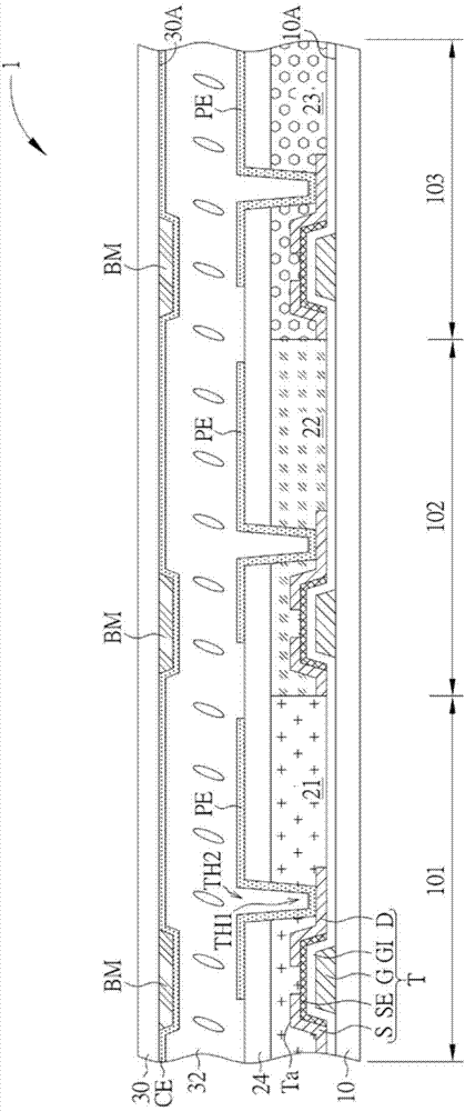
[0040] Please refer to figure 1 . figure 1 A schematic diagram of a display panel of a comparative example of the present invention is shown. Such as figure 1As shown, the display panel 1 of the comparative embodiment includes a first substrate 10, a plurality of thin film transistor elements T, a first color filter layer 21, a second color filter layer 22, a third color filter layer 23, and a plurality of pixels The electrode PE, the second substrate 30 , the photoelectric medium layer 32 , the black matrix BM and the common electrode CE. The first substrate 10 is an array substrate, which can be a transparent substrate such as a...


PUM


Abstract

The present invention provides a display panel and a manufacturing method thereof. The display panel comprises a substrate, a plurality of thin film transistor elements, a plurality of color filter layers with different colors, and a plurality of auxiliary color filtering patterns. The thin film transistor elements and the color filter layers are disposed on the substrate and positioned in corresponding pixel areas, and each color filter layer is provided with an opening to expose the corresponding thin film transistor element. The auxiliary color filtering patterns are respectively disposed in the openings of the color filter layers and have the same light penetrating wave length frequency spectrum. The color filter layers of the display panel are disposed on the array substrate, and therefore the opening ratio can be effectively improved. In addition, the auxiliary color filtering patterns having the same color are covered over the thin film transistor elements in the pixel areas used for display different colors, so that leakage currents of all the thin film transistor elements are identical, and the thin film transistor elements have consistent element characteristics without color cast.

Description

technical field [0001] The present invention relates to a display panel and a manufacturing method thereof, in particular to a display panel with high aperture ratio and low color shift and a manufacturing method thereof. Background technique [0002] A display panel such as a liquid crystal display panel is usually composed of an array substrate (Array substrate) and a color filter substrate (Color Filter substrate, CF substrate). The array substrate is provided with thin film transistor elements and peripheral circuits, and the color filter substrate A color filter layer such as a red filter layer, a green filter layer and a blue filter layer is disposed on the substrate. Due to the deviation of the array substrate and the color filter substrate in the process of grouping, it is necessary to increase the width of the black matrix (BM) to avoid light leakage caused by the deviation of the group, but the increase in the width of the black matrix will make the light transmiss...

Claims


Application Information

Patent Timeline
Patent Type & Authority Applications(China)
IPC IPC(8): G02F1/1335G02F1/1333
CPCG02F1/1333G02F1/133514G02F1/1362G02F1/133357G02F1/136222G02F1/133512H01L27/1214H01L27/1262H04N9/12
Inventor 陈耀铭沈柏元陈家芳
Owner AU OPTRONICS CORP
Why Eureka
Try Eureka