Manufacturing method of memory apparatus, memory device and memory apparatus

A technology for storage devices and manufacturing methods, applied in static memory, digital memory information, information storage, etc., can solve problems such as small size or interval, difficulty in obtaining element characteristics, and changes in contact area, so as to achieve improved element characteristics and consistent element characteristics , reducing the effect of misalignment

Inactive Publication Date: 2012-05-16
SONY SEMICON SOLUTIONS CORP
View PDF11 Cites 0 Cited by
  • Summary
  • Abstract
  • Description
  • Claims
  • Application Information

AI Technical Summary

Problems solved by technology

[0006] However, there is a problem in the prior art that uniform element characteristics are difficult to obtain due to variations in the contact area between the lower electrode and the storage layer due to misalignment of the storage layer and the upper electrode with respect to the lower electrode.
Especially in the case of high-density memory devices, since it is desired to form the lower electrodes with a size or spacing as small as possible, the change in the contact area between the lower electrodes and the storage layer caused by misalignment becomes a more serious problem.

Method used


Image

  • Manufacturing method of memory apparatus, memory device and memory apparatus
  • Manufacturing method of memory apparatus, memory device and memory apparatus
  • Manufacturing method of memory apparatus, memory device and memory apparatus

Examples


no. 1 example

[0035] 1. First embodiment (example in which the planar shape of the lower electrode is a quadrilateral)

[0036] 2. Second embodiment (example in which insulating side walls are provided on the same side of two opposite sides of a quadrangle)

[0037] 1. The first embodiment

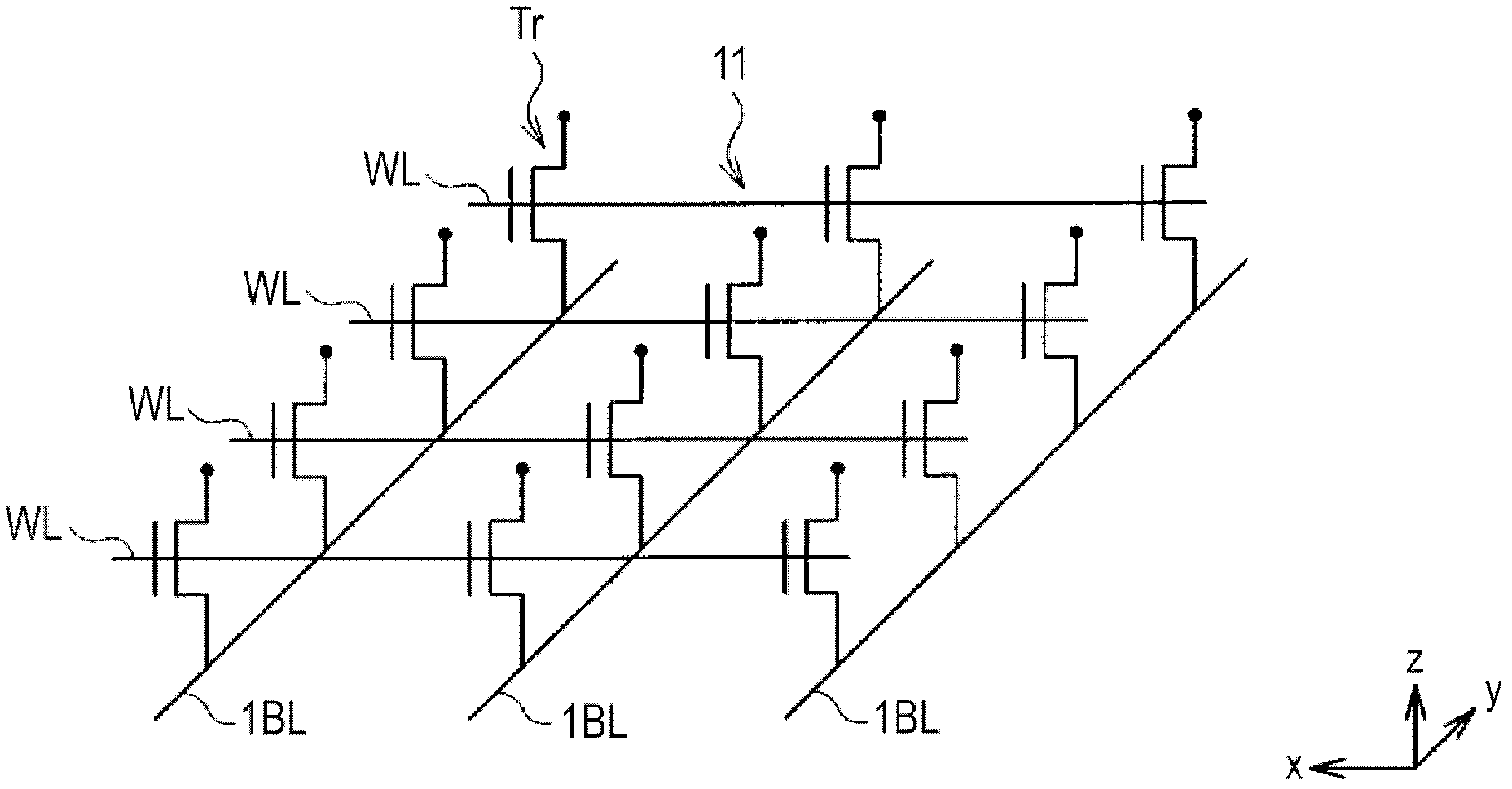
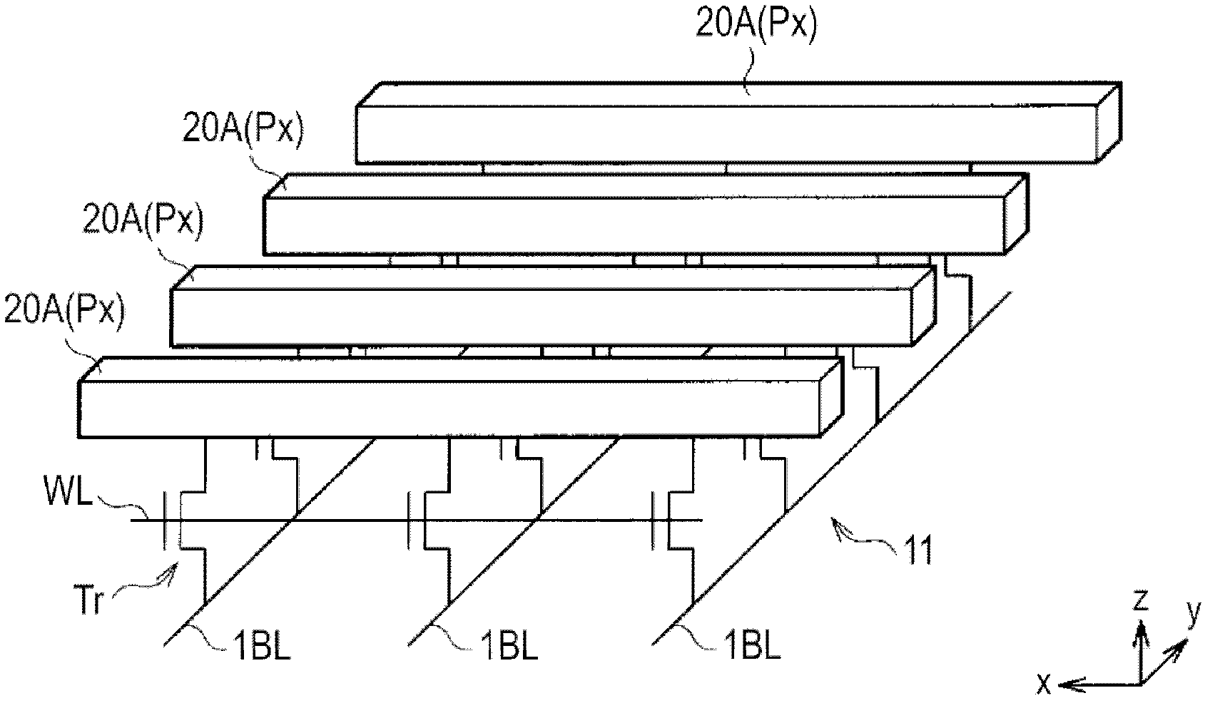
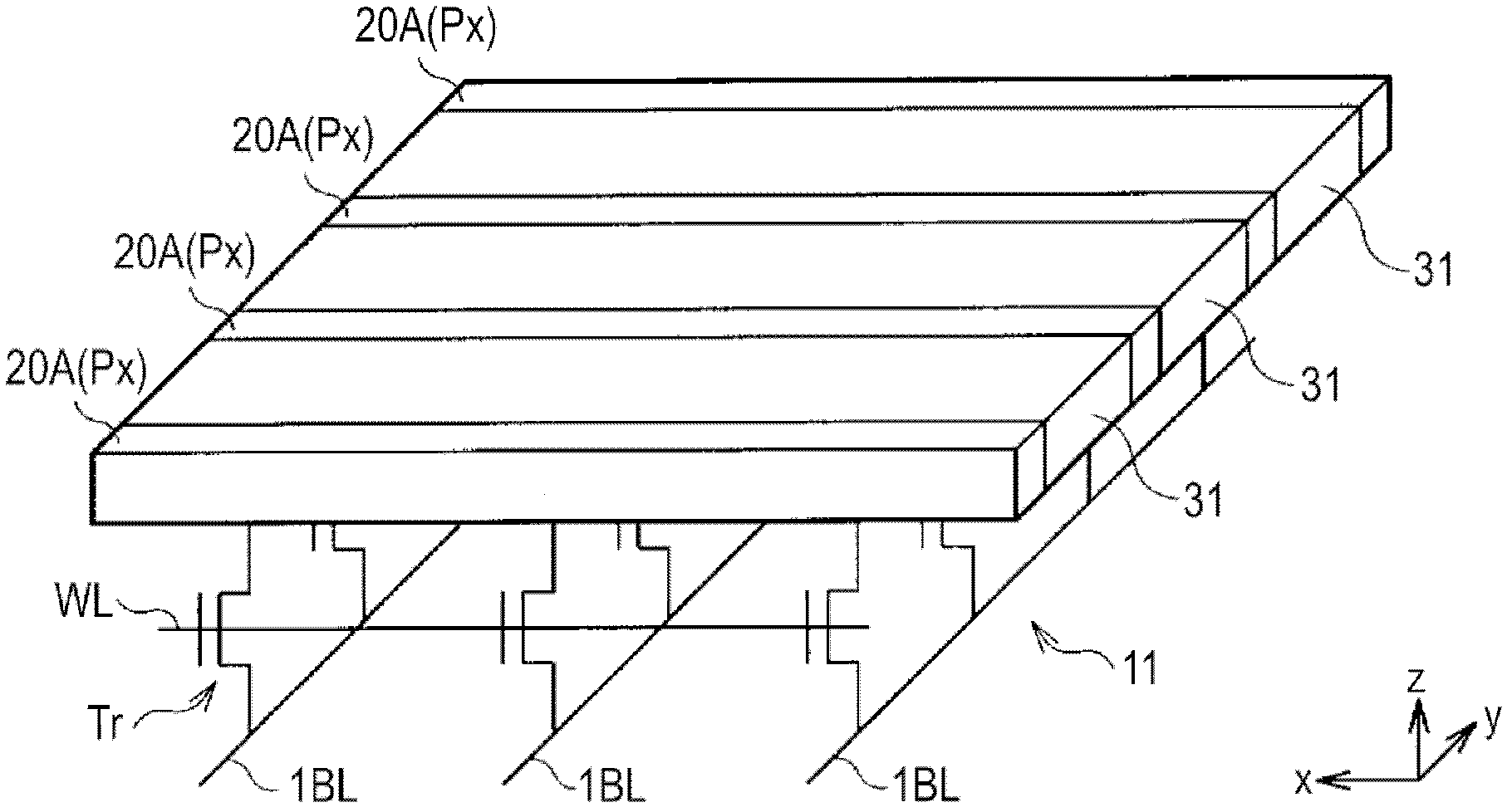
[0038] Figure 1-Figure 6 and Figure 12 The manufacturing method of the storage device according to the first embodiment of the present invention is shown in order of procedures. First, if figure 1 As shown, on the substrate 10 ( figure 1 not shown, see Figure 7 ) to form a transistor array 11, and the substrate 10 is a silicon wafer or the like. In the transistor array 11, the first bit lines 1BL and the word lines WL are formed in a matrix state, and at the same time, the transistors Tr are arranged at intersections of the first bit lines 1BL and the word lines WL. One of the source and the drain of the transistor Tr is connected to a lower electrode 20 (to be described later) of each memory ...


PUM


Abstract

A manufacturing method of a memory apparatus in which memory devices each having a memory layer whose resistance value reversibly varies by voltage application between bottom and upper electrodes are formed, includes: forming and shaping a bottom electrode material film into a first linear pattern extending in a first direction; forming a memory layer material film and an upper electrode material film in this order on the bottom electrode material film; forming the upper electrodes and the memory layers by shaping the upper electrode material film and the memory layer material film into a second linear pattern extending in a second direction intersecting with the first direction; and forming the bottom electrodes having a quadrangle plane shape at regions where the first linear pattern intersect with the second linear pattern by shaping the bottom electrode material film into the second linear pattern.

Description

[0001] Cross References to Related Applications [0002] The present invention contains subject matter related to the disclosure of Japanese Priority Patent Application JP 2010-234414 filed in the Japan Patent Office on Oct. 19, 2010, the entire content of which is hereby incorporated by reference. technical field [0003] The present invention relates to a method of manufacturing a storage device including a storage device capable of storing information through changes in electrical characteristics of a storage layer, a storage device, and a storage device. Background technique [0004] In recent years, active efforts have been made to develop a 1T1R type nonvolatile memory that combines a so-called resistance change type memory device that records a low-resistance / high-resistance state by applying an electrical pulse, with a transistor array. [0005] For the manufacturing method of the resistance variable memory device, in the prior art (for example, refer to the internat...

Claims


Application Information

Patent Timeline
Patent Type & Authority Applications(China)
IPC IPC(8): H01L45/00H01L27/24
CPCH01L45/1266H01L27/2436H01L45/141H01L45/146H01L45/085H01L45/06H01L27/2472H01L45/1233H10B63/82H10B63/30H10N70/245H10N70/8416H10N70/826H10N70/8833G11C13/0002H10N70/068H10N70/8828
Inventor 宫田幸児
Owner SONY SEMICON SOLUTIONS CORP
Why Eureka
Try Eureka