Sic single-crystal substrate and method of producing sic single-crystal substrate

a single crystal substrate and crystal technology, applied in the direction of crystal growth process, polycrystalline material growth, chemistry apparatus and processes, etc., can solve the problems of substrate defects, device property stability and yield would still be inadequate for achieving wide utilization, and achieve stable electrical properties and high yield

Active Publication Date: 2010-11-25
SHOWA DENKO KK
View PDF1 Cites 41 Cited by
  • Summary
  • Abstract
  • Description
  • Claims
  • Application Information

AI Technical Summary

Benefits of technology

[0030]In the present invention, dislocations in the crystal can be aggregated or annihilated at proximal locations by moving them under high-temperature condition. In a substrate cut and processed from a crystal produced in accordance with the

Problems solved by technology

As pointed out in the foregoing, although devices using SiC crystal substrates are viewed as promising next-generation power devices to replace the current Si generation, they are inadequate in the stability of device properties and poor in yield.
The primary reason for this is substrate defects, particularly micropipes.
However, it is believed that even if substrates totally free of micropipes should be used, device property s

Method used


Image

  • Sic single-crystal substrate and method of producing sic single-crystal substrate
  • Sic single-crystal substrate and method of producing sic single-crystal substrate
  • Sic single-crystal substrate and method of producing sic single-crystal substrate

Examples


example 1

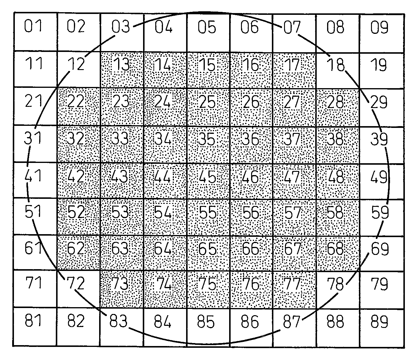
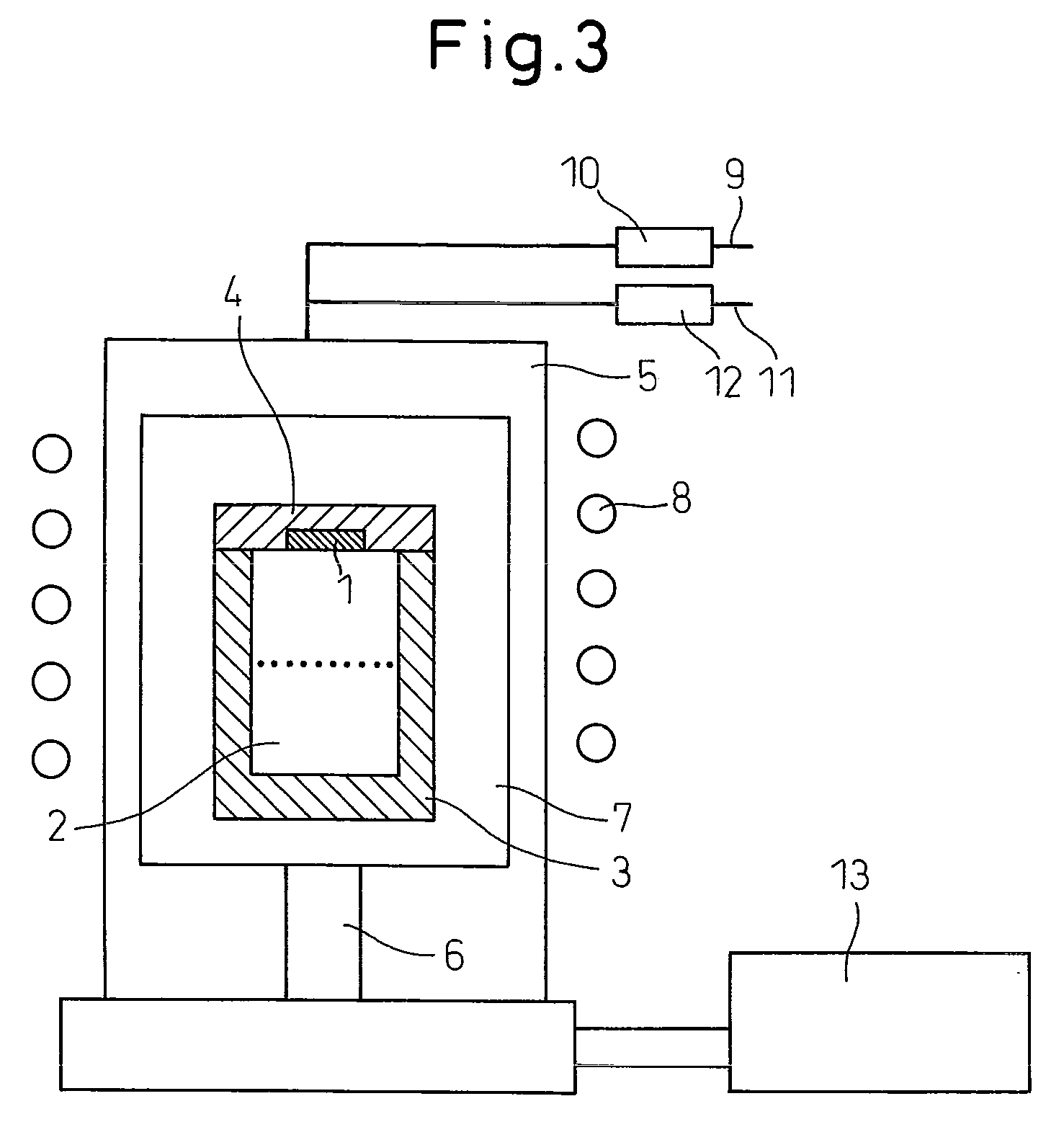
[0048]A single crystal production apparatus for producing the invention single crystal, such as shown in FIG. 3, was used to produce single crystal. A 52 mm diameter 4H SiC single-crystal substrate having a {0001} surface was prepared as seed crystal. A seed crystal was cut from the crystal, which had a total dislocation density of about 12,000 / cm2, and then machined. Next, the seed crystal 1 was attached to the inner surface of the graphite crucible lid 4 of a graphite crucible 3. Powdery SiC crystal raw material 2 was charged into the graphite crucible 3 after cleansing.

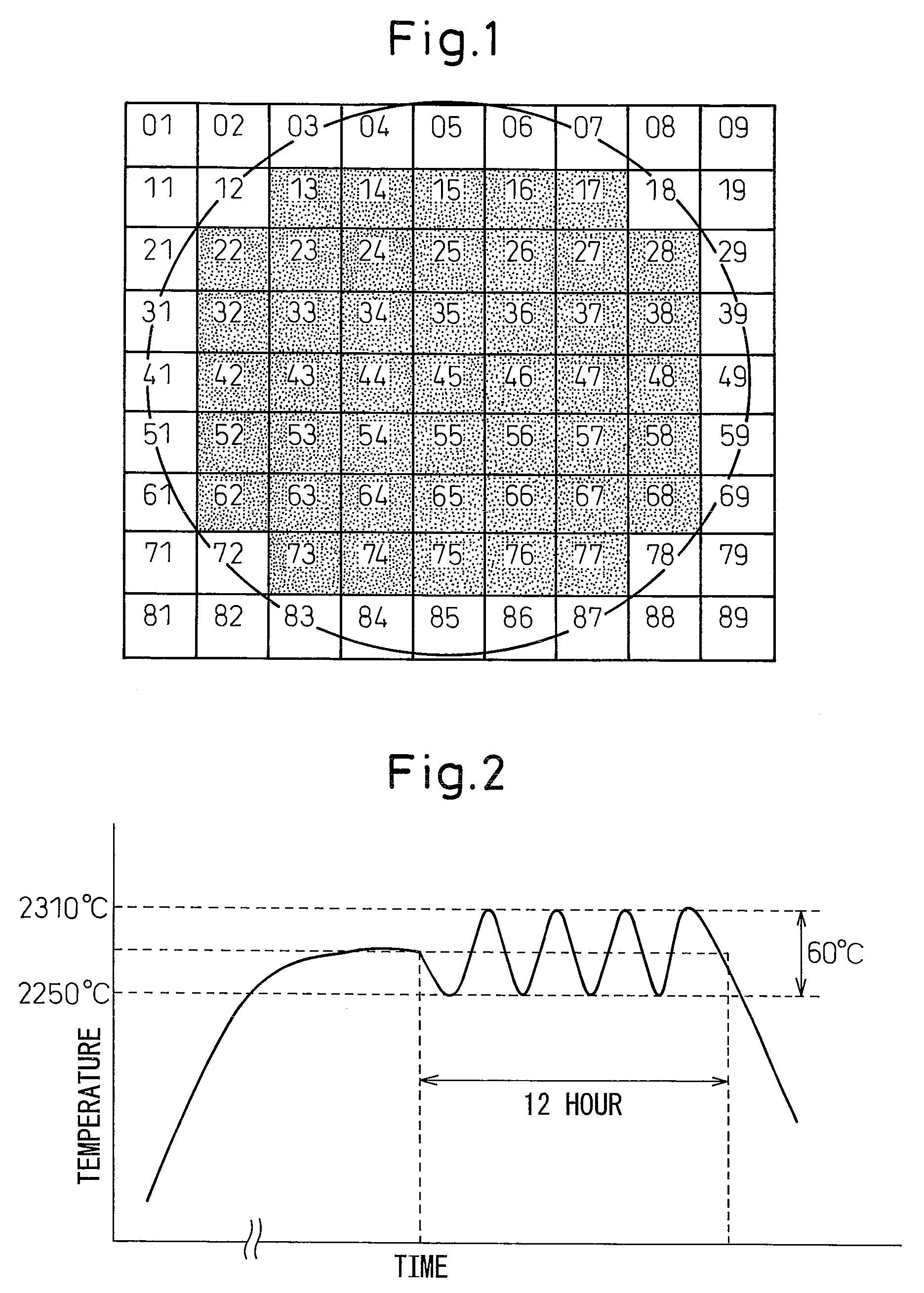
[0049]Next, the graphite crucible 3 charged with the raw material was closed with the graphite crucible lid 4, wrapped in graphite felt 7, and placed on a graphite pedestal 6 inside a dual-wall quartz sheath 5. The interior of the quartz sheath was evacuated with a vacuum pumping unit 13 and then supplied with an atmosphere gas composed of a mixed gas of high-purity Ar gas mixed with about 7% nitrogen gas obtained ...

example 2

[0052]Crystal growth was conducted similarly to in Example 1 using a large diameter crucible and a substrate of 70-mm diameter size as a seed crystal. The total dislocation density of the seed crystal was about 10,000 / cm2. Between the fifth to tenth hour of crystal growth, thermal cycling treatment consisting of 5 temperature cycles within a 60° C. range was conducted similarly to in Example 1. Observation of dislocation distribution by the same method as in Example 1 revealed presence of dislocation pairs and / or dislocation rows in 32% of the regions. The average dislocation density of the regions having no dislocation pairs or dislocation rows was 5,000 / cm2. The substrate measured about 72-mm in diameter.

example 3

[0053]Crystal was produced by the same method as set out in Example 1. A substrate cut from the crystal was polished, and an approximately 10-μm thick SiC single crystal film was grown on the substrate surface in 2 hr using a commercially available CVD epitaxial growth system for SiC.

[0054]The epitaxial film was grown on a substrate whose plane orientation was inclined by 4° from . Its surface dislocation distribution was observed as set out in Example 1. Dislocation pairs and / or dislocation rows were found to be present in 10% of the regions. The average dislocation density of the regions having no dislocation pairs or dislocation rows was 4,000 / cm2. The ratio of regions with dislocation pairs and or dislocation rows was on substantially the same level as the dislocation distribution of the substrate. Although a small increase was seen in the dislocation density of portions with no dislocation rows, the level was substantially the same.


PUM


Abstract

The invention provides a high-quality SiC single-crystal substrate, a seed crystal for producing the high-quality SiC single-crystal substrate, and a method of producing the high-quality SiC single-crystal substrate, which enable improvement of device yield and stability. Provided is an SiC single-crystal substrate wherein, when the SiC single-crystal substrate is divided into 5-mm square regions, such regions in which dislocation pairs or dislocation rows having intervals between their dislocation end positions of 5 μm or less are present among the dislocations that have ends at the substrate surface account for 50% or less of all such regions within the substrate surface and the dislocation density in the substrate of dislocations other than the dislocation pairs or dislocation is 8,000/cm2.

Description

FIELD OF THE INVENTION[0001]The present invention relates to a SiC single-crystal and a method of producing the same.BACKGROUND ART[0002]SiC semiconductors utilizing SiC single-crystal are viewed as promising candidates for next-generation power devices to replace Si transistors. Applications as substrates for blue light-emitting diodes and laser diodes are also expected.[0003]In addition to being physically and chemically stable, SiC single-crystal is a material that can withstand high temperature and radiation. It is therefore thought to have potential for application as an environment-resistant semiconductor material. Moreover, SiC power devices are also attracting attention, particularly as energy-saving devices, because the power loss in the device can be reduced greatly in comparison with that in a conventional Si device.[0004]However, no crystal growth technology has yet been established that can provide a stable supply of high-quality SiC single crystal of large surface area...

Claims


Application Information

Patent Timeline
IPC IPC(8): H01L29/24H01L21/20
CPCC30B23/00C30B29/36H01L21/02631H01L21/02529H01L21/02378
Inventor FUJIMOTO, TATSUOTATSUMI, KOHEIHOSHINO, TAIZOKATSUNO, MASAKAZUOHTANI, NOBORUNAKABAYASHI, MASASHITSUGE, HIROSHIHIRANO, HOUSEIYASHIRO, HIROKATSU
Owner SHOWA DENKO KK
Why Eureka
Try Eureka