

High voltage junction field effect transistor
a high-voltage junction and transistor technology, applied in the field of semiconductor devices, can solve the problems of easy slipping of the voltage, and achieve the effect of reducing the sensitivity to process variation
- Summary
- Abstract
- Description
- Claims
- Application Information
AI Technical Summary
Benefits of technology
Problems solved by technology
Method used
Image

Examples
first embodiment
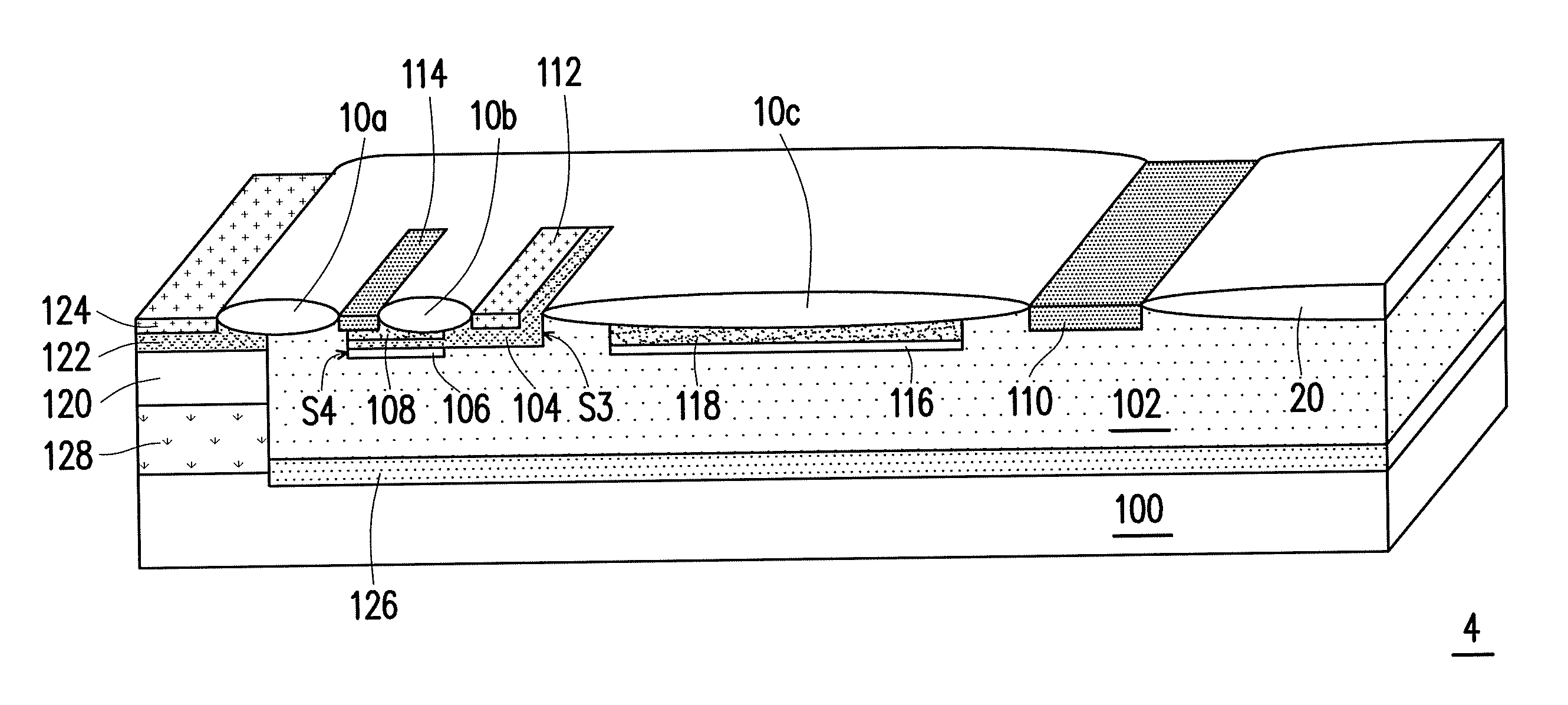
[0037]FIG. 1 is a schematic top view of a semiconductor device according to the invention.
[0038]With reference to FIG. 1, the invention provides a semiconductor device 1, which includes: a substrate 100, a well region 102 of a first conductivity type, a plurality of top doped regions 116 of a second conductivity type, a first doped region 110 of the first conductivity type, a field region 104 of the second conductivity type, and a second doped region 112 of the second conductivity type. The substrate 100 is a semiconductor substrate of the first conductivity type, e.g., a P-type substrate, for example. A material of the semiconductor substrate is at least one selected from a group consisting of Si, Ge, SiGe, GaP, GaAs, SiC, SiGeC, InAs, and InP, for example. The substrate 100 may also be an EPI layer, a non-EPI layer, a silicon on insulator (SOI) substrate, or a combination of the foregoing, for example.
[0039]The well region 102 is located in the substrate 100. Although FIG. 1 illus...
second embodiment
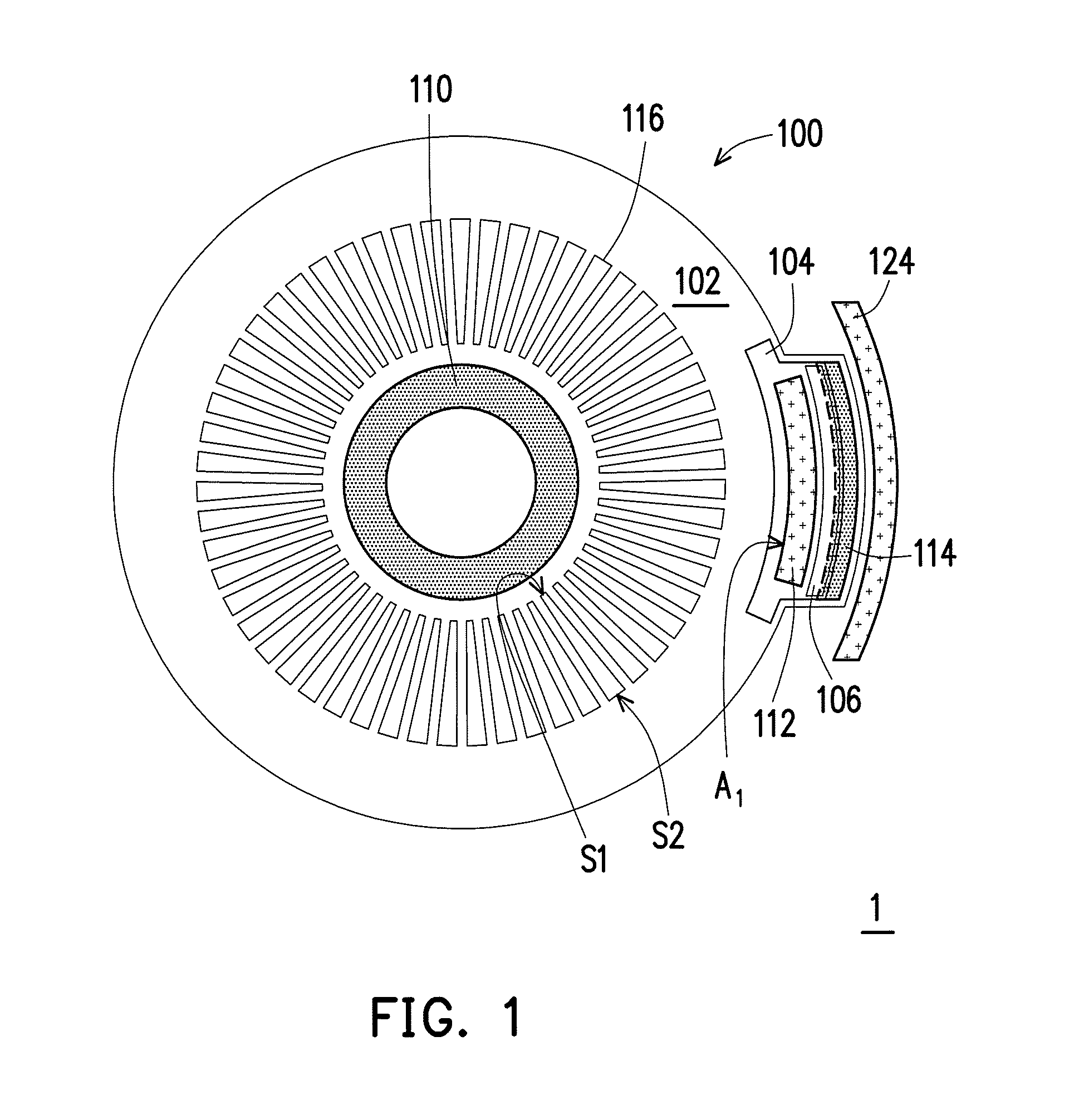
[0043]FIG. 2 is a schematic top view of a semiconductor device according to the invention.
[0044]With reference to FIG. 1 and FIG. 2, a semiconductor device 2 of the second embodiment is similar to the semiconductor device 1 of the first embodiment of the invention, and a difference therebetween lies in that: the semiconductor device 2 of the second embodiment includes two field regions 104a and 104b, two second doped regions 112a and 112b, two third doped regions 114a and 114b, two top doped regions 106a and 106b, and two fourth doped regions 124a and 124b. In FIG. 2, the field regions 104a and 104b, the second doped regions 112a and 112b, the third doped regions 114a and 114b, the top doped regions 106a and 106b, and the fourth doped regions 124a and 124b are arranged symmetrically with respect to the first doped region 110. Nevertheless, the invention is not limited thereto. In other embodiments, the foregoing doped regions are arranged asymmetrically with respect to the first dop...
third embodiment
[0045]FIG. 3 is a perspective cross-sectional view of a semiconductor device according to the invention. FIG. 4 is a schematic cross-sectional view along the line A-A′ of FIG. 3. FIG. 5 is a schematic cross-sectional view along the line B-B′ of FIG. 3.
[0046]With reference to FIG. 3, FIG. 4, and FIG. 5, the invention provides a semiconductor device 3, which includes: a substrate 100 of a second conductivity type, a well region 102 of a first conductivity type, a field region 104 of the second conductivity type, a first doped region 110 of the first conductivity type, a second doped region 112 of the second conductivity type, a third doped region 114 of the first conductivity type, a top doped region 106 of the second conductivity type, and an insertion layer 108 of the first conductivity type. The material of the substrate 100 has been specified in the above embodiment and thus is not repeated hereinafter.
[0047]The well region 102 is located in the substrate 100. In an embodiment, a ...
PUM
 Abstract
Description
Claims
Application Information