Use of redundant routes to increase the yield and reliability of a VLSI layout

a technology of vlsi layout and redundant route, which is applied in the direction of cad circuit design, program control, instruments, etc., can solve the problems of previously existing redundant vias that must be maintained, second paths previously existing redundant vias may only be inserted, so as to increase the reliability of integrated circuit inter, reduce manufacturing defects, and reduce redundancy

Active Publication Date: 2007-12-11
GLOBALFOUNDRIES US INC
View PDF25 Cites 211 Cited by
  • Summary
  • Abstract
  • Description
  • Claims
  • Application Information

AI Technical Summary

Benefits of technology

[0004]This invention provides an automated method for reducing integrated circuit design sensitivity to manufacturing defects and increasing integrated circuit reliability by using existing router technology (e.g., routing programs) to increase redundancy of inter-layer connectors (i.e., vias) and intra-layer connectors (e.g., wire segments) in order to enhance circuit reliability and yield. Once the initial routing is completed, single vias (i.e., a single via used to make an inter-layer connection) are identified. Then, a specific single via is selected and temporarily blocked. Specifically, the selected single via is marked within the routing program as not available for connecting a first element (e.g., a wire, pin, device, etc.) to a second element (e.g., a wire, pin, device, etc.). The single via is also preferably coded as “must keep” so that the routing program will not remove the original single via in order to form another path. Then, the existing routing program identifies an available alternate route for a connection between the first and second elements and inserts a second path therein. The second path comprises a loop that extends from the first element to the second element and comprises at least one additional via and an additional intra-layer connector (e.g., wire segment). Once the second path is inserted, the single via is unblocked. Thus, the first element and the second element are connected by both first and second paths (i.e., redundant paths). The process is repeated for each single via identified. These redundant paths are used to reduce the integrated circuit's sensitivity to manufacturing defects that may be caused by a potential block in the single via.
[0009]This invention also provides a system for reducing sensitivity to manufacturing defects and increasing reliability in integrated circuit inter and intra-layer connections. The system comprises a router for identifying available routes and for inserting intra-layer connectors (e.g., wire segments) and inter-layer connectors (i.e., vias) into the available routes to form connecting paths. An identifier identifies single vias in previously routed connecting paths, e.g., a single via in a first path connecting a first element (e.g., wire, pin, device, etc.) and a second element (e.g., wire, pin, device, etc.). A diverter blocks a selected single via so that it is not recognized by the router as a connection between a first element and second element. The diverter must also make sure that the router does not remove possibly created antennas, e.g. by setting all remaining connections of the net to “must keep.” In other words, the diverter tricks the router into proceeding as if the single via is not available for use in connecting the first element to the second element. The router is further adapted to determine an alternate path (i.e., second path) for connecting a first element and a second element when the single via is blocked and for inserting the path. The diverter is further adapted for unblocking the selected single via once the second path is inserted such that the first path and the second path provide redundant paths between the first element and the second element. A controller controls the router by placing limitations on the second path which may be used. For example, the controller may be adapted to restrict the second path to within an area between and within the metal layers used by the first path and / or to within a predetermined distance from the single via. The controller may also restrict the router from ripping up existing vias in order to form the second path. Additionally, the controller may be adapted to conduct a cost-benefit analysis and to only insert the second path if a benefit of inserting the second path outweighs a cost of inserting the second path.
[0010]Therefore, the invention provides a method for inserting redundant paths into integrated circuit wiring. A redundant path provides greater redundancy than a redundant via alone. Additionally, a redundant path provides for redundancy when congestion prevents a redundant via from being inserted. This redundancy enhances circuit yield and reliability by reducing the probability of failures due to random defects. These, and other, aspects and objects of the present invention will be better appreciated and understood when considered in conjunction with the following description and the accompanying drawings. It should be understood, however, that the following description, while indicating preferred embodiments of the present invention and numerous specific details thereof, is given by way of illustration and not of limitation. Many changes and modifications may be made within the scope of the present invention without departing from the spirit thereof, and the invention includes all such modifications.

Problems solved by technology

For example, one limitation may be that the second path may only be inserted if it is located within and between those metal layers used by the first path.
Another limitation may be that the second path may only be inserted if is inside a predetermined distance from the single via and / or it is outside another predetermined distance from said single via.
Yet another limitation may be that any previously existing redundant vias must be maintained when inserting a second path.
Inserting a redundant path (i.e. a second path) reduces the probability that an open circuit fault will occur by reducing the open circuit fault critical area within the integrated circuit (e.g., within the integrated circuit wiring), but also increases the probability of a random short circuit fault by increasing the short circuit fault critical area in the integrated circuit (e.g., within the integrated circuit wiring).

Method used


Image

  • Use of redundant routes to increase the yield and reliability of a VLSI layout
  • Use of redundant routes to increase the yield and reliability of a VLSI layout
  • Use of redundant routes to increase the yield and reliability of a VLSI layout

Examples


Embodiment Construction

[0027]The present invention and the various features and advantageous details thereof are explained more fully with reference to the non-limiting embodiments that are illustrated in the accompanying drawings and detailed in the following description. It should be noted that the features illustrated in the drawings are not necessarily drawn to scale. Descriptions of well-known components and processing techniques are omitted so as to not unnecessarily obscure the present invention. The examples used herein are intended merely to facilitate an understanding of ways in which the invention may be practiced and to further enable those of skill in the art to practice the invention. Accordingly, the examples should not be construed as limiting the scope of the invention.

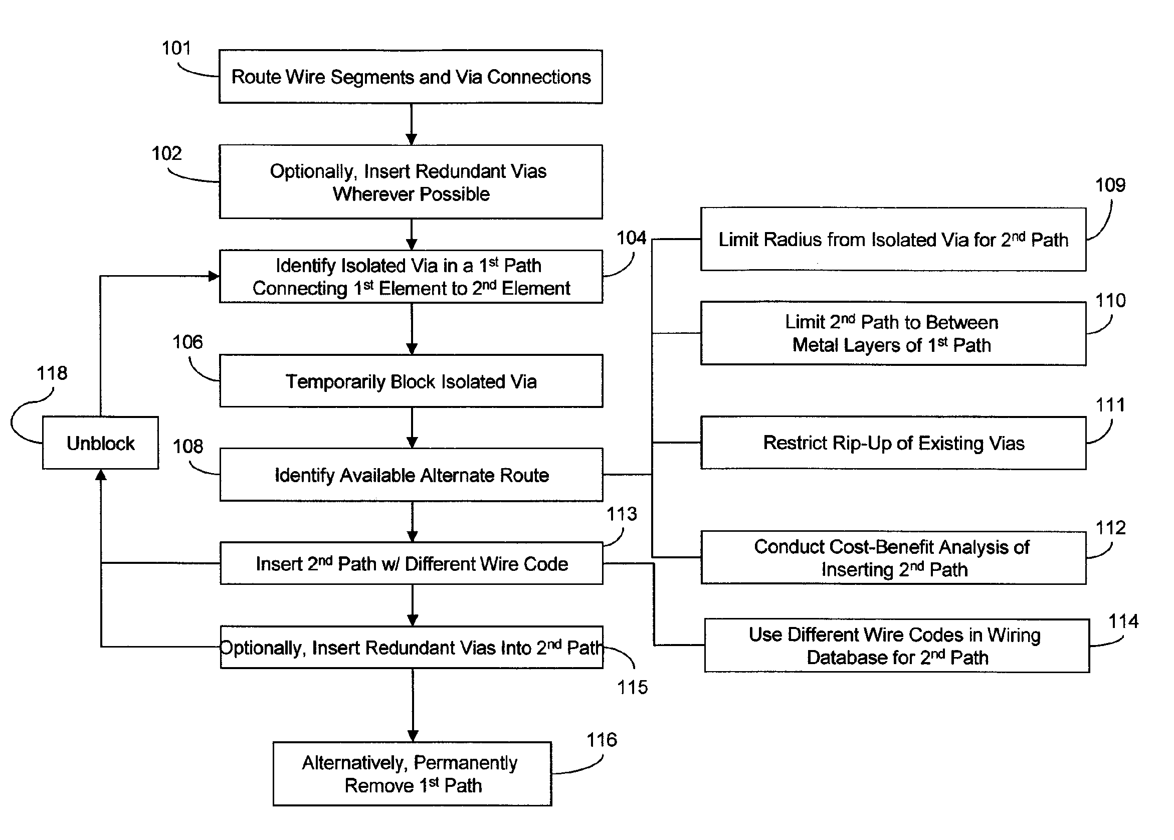
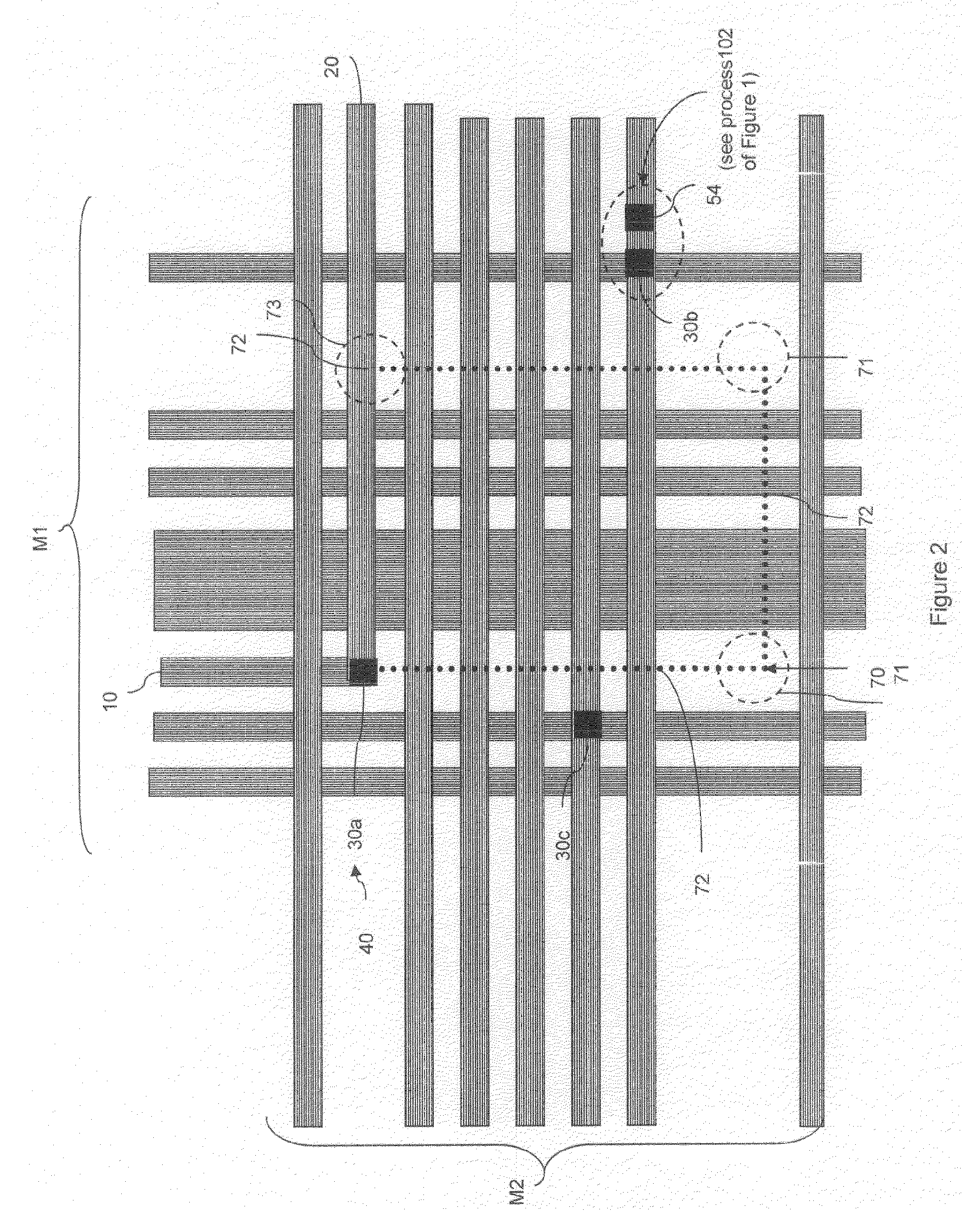
[0028]The invention relates to integrated circuits and, in particular, to a method for increasing redundancy in routed very large scale integration (VLSI) designs in order to enhance circuit yield and reliability. The metho...


PUM


Abstract

Disclosed is a method and system for inserting redundant paths into an integrated circuit. Particularly, the invention provides a method for identifying a single via in a first path connecting two elements, determining if an alternate route is available for connecting the two elements (other than a redundant via), and for inserting a second path into the available alternate route. The combination of the first and second paths provides greater redundancy than inserting a redundant via alone. More importantly, such redundant paths provide for redundancy when congestion prevents a redundant via from being inserted adjacent to the single via. An embodiment of the method further comprises removing the single via and any redundant wire segments, if all of the additional vias used to form the second path can be made redundant.

Description

FIELD OF THE INVENTION[0001]The invention relates to integrated circuits and in particular, to a method for increasing redundancy in routed very large scale integration (VLSI) designs in order to enhance circuit reliability.DESCRIPTION OF THE RELATED ART[0002]As the physical dimensions of very large scale integrated circuits (VLSI) continue to shrink, it has become increasingly difficult to manufacture such integrated circuits reliably. The sensitivity of a VLSI design to random defects increases as feature widths and spacing between features grow smaller. In addition, the presence of single vias (i.e., inter-layer connectors through a single via) is particularly undesirable. From the perspective of random-defect yield, a single via is especially likely to cause a chip failure because a spot defect landing on a single via will create an open circuit. From the perspective of systematic yield, if vias are difficult to manufacture in a given process, then a poorly created single via ca...

Claims


Application Information

Patent Timeline
Patent Type & Authority Patents(United States)
IPC IPC(8): G06F17/50
CPCG06F17/5077G06F17/5068G06F30/39G06F30/394
Inventor BUEHLER, MARKUS T.COHN, JOHN M.HATHAWAY, DAVID J.HIBBELER, JASON D.KOEHL, JUERGEN
Owner GLOBALFOUNDRIES US INC
Why Eureka
Try Eureka