Ambient light rejection for non-imaging contact sensors

a contact sensor and ambient light technology, applied in the field of non-imaging contact sensors, can solve the problems of fingerprint contact sensors that cannot be used in fingerprint scanners, fingerprint contact sensors that are saturated and lost, and commercially useful non-imaging contact fingerprint sensors that have not been successfully developed for use in fingerprint scanners, etc., to achieve the effect of reducing the effect of ambient ligh

Active Publication Date: 2013-05-16
HID GLOBAL CORP
View PDF10 Cites 206 Cited by
  • Summary
  • Abstract
  • Description
  • Claims
  • Application Information

AI Technical Summary

Benefits of technology

[0011]Accordingly, one object of the present invention is to provide non-imaging contact sensors which reduce the amount of, or blocks, ambient light upon light sensing pixel elements of the sensors.
[0012]It is another object of the present invention to provide non-imaging contact sensors which block or reduce ambient light when present so as to improve imaging by such sensors when utilized in fingerprint or other skin topology scanners.
[0015]Briefly described, the present invention embodies a sensor for capturing images of skin topology, such as one or more fingers, having a platen, a one or two-dimensional array of light sensing pixel elements for receiving light representative of skin topology of skin when present upon the platen, and one of more structures or layers of material for reducing or blocking ambient light which would hinder the light sensing pixel elements from sensing the light representative of skin topology.
[0019]In operation, only a portion (active area) of the overall area of each of the light sensing pixel elements receives the light representative of skin topology. Optionally, this portion with respect to the overall each of each light sensing pixel element is selected in the sensor to reduce the amount of ambient illumination received by the array when such ambient illumination is present in relation to the amount of desired light illuminating the platen. Although this reduction of the active area of the pixel elements may reduce sensor array sensitivity to light representative of skin topology, it has the benefit of reducing the risk of light sensing elements becoming saturated by ambient light if present in amount which otherwise saturate the sensing elements. For the case of a non-imaging contact sensor that is constructed on a transparent backplane, reduction in the pixel active area allows for more of the pixel element to be transparent, thereby enabling more light in the case of backside illumination to preferably illuminate the platen surface as opposed to ambient light that might be present. Preferably, the percentage of the active area with respect to the overall area of each light sensing pixel element is less than 40% as compared to typical TFT-based light detecting sensors used in X-ray devices that strive for 80-100% active area. To achieve such high active area percentages in TFT-based digital X-ray devices, sometimes requires the electronics of the pixel (e.g., transistors) to be placed underneath the photodiode of the pixel. Although the pixel electronics of the present invention are illustrated in the Figures as being next to the light sensitive portion of the pixel, it is understood that the electronics may also be underneath the photodiodes, thereby enabling even more of the pixel area to be transparent, thereby further increasing the amount of desired light in ratio to ambient light that is detected. Such selected reduction of the pixel active area may be provided with or without the above described structure(s) or layer(s) of material disposed in the path of ambient light for reducing or blocking ambient light.

Problems solved by technology

However, heretofore the improvements provided by the present invention, a commercially useful non-imaging contact fingerprint sensor has not been successfully developed for use in fingerprint scanners.
It has been found that fingerprint images taken with a TFT-based non-imaging contact sensor of the type depicted in FIG. 2 with the room lights “off” provides an adequate fingerprint image, however when ambient light provided by room lights that are “on” is present, a significant amount of fingerprint image becomes saturated and lost.
Such saturation worsens for fingerprint contact sensors that operate with outdoor ambient illumination, rather than room (artificial) light ambient illumination, since sunlight as generally significantly higher intensity than room light.

Method used


Image

  • Ambient light rejection for non-imaging contact sensors
  • Ambient light rejection for non-imaging contact sensors
  • Ambient light rejection for non-imaging contact sensors

Examples


first embodiment

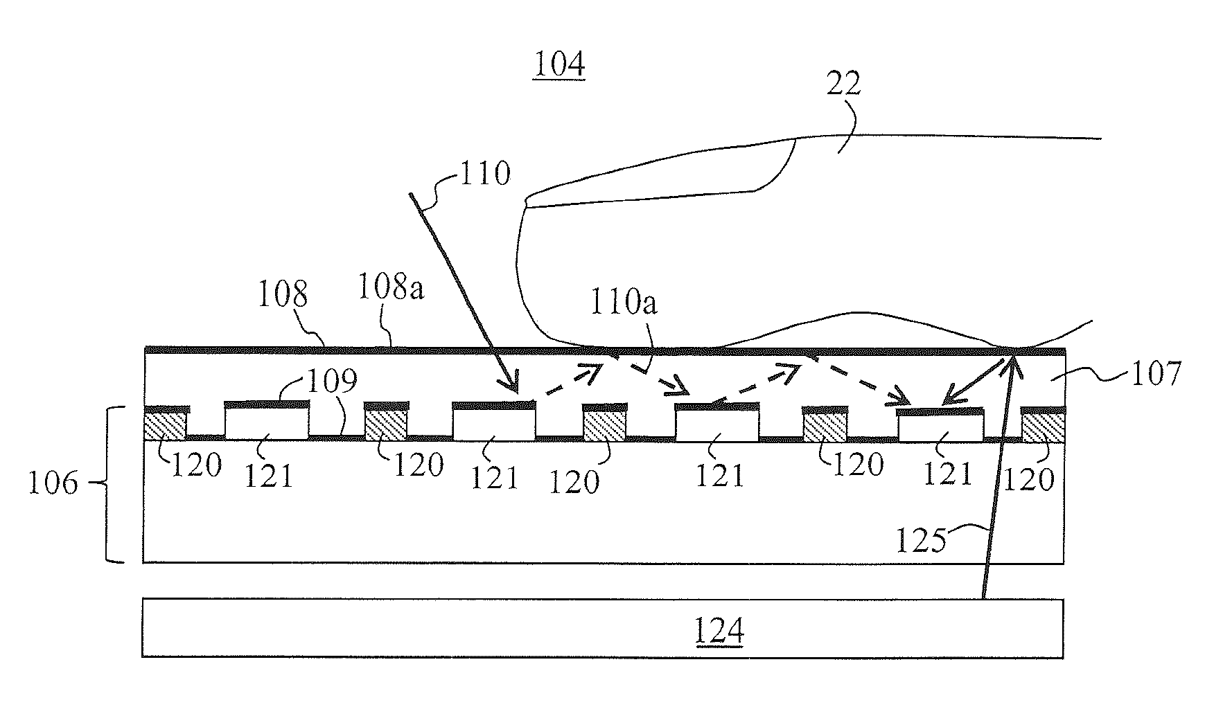
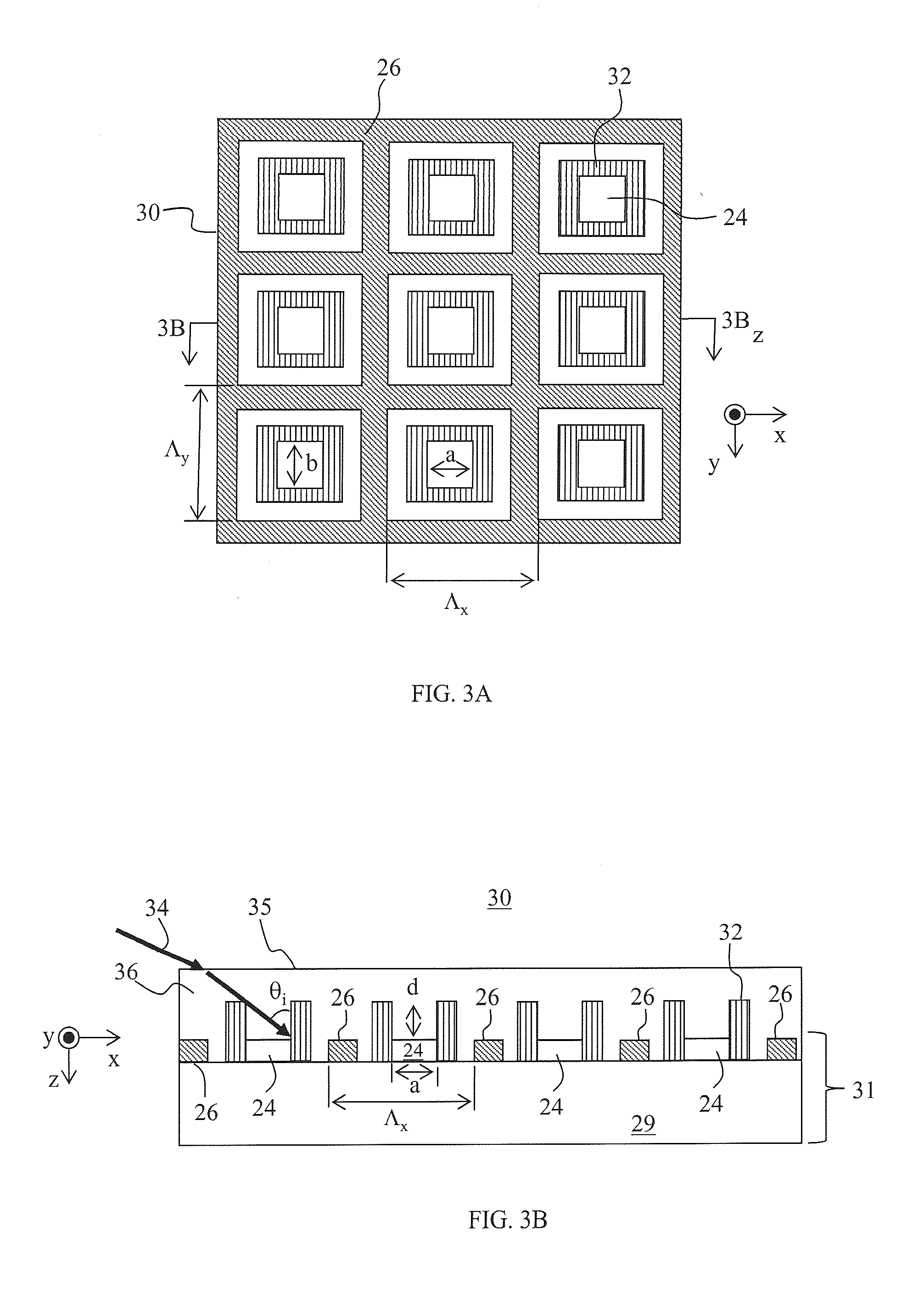
[0039]Referring to FIGS. 3A and 3B, a non-imaging contact sensor 30 in accordance with the present invention is shown having a two-dimensional array 31 of light sensing pixel elements (or pixels) 24 which is the same or similar as shown in array 20a as described earlier with the improvement of each light sensing pixel 24 having a light barrier (or wall) 32 surrounding its photosensitive region or area. Each light barrier 32 may be constructed of material(s) that are opaque to at least some of the wavelengths the light sensing pixel 24 is sensitive to and such light barrier 32 extends above the photosensitive region a distance “d” and barrier 32 helps restrict ambient light 34 from being detected by the light sensing region 24 of width “a” and height “b”. In such a manner, as illustrated in the x-z plane of FIG. 4B, light that propagates at an angle of θi is blocked from exposing the light sensing pixel 24. By way of example if the width of the light sensitive region 24 in the x dire...

second embodiment

[0045]However, in accordance with the present invention for fingerprint scanning applications, the reverse of the current trend for high fill factor is provided, namely that because of the possibility of the light sensing regions 24 being saturated by ambient light and because a TFT sensor for fingerprint scanning may be backlit (as opposed to digital X-ray applications where the sensor is always front lit), that the fill factor of the sensor array may be purposely reduced and in fact be in the region of <40%, or even <30% or <20% if needed to reduce the amount of ambient illumination received by the sensor array when such ambient illumination is present despite the loss of sensor array sensitivity. Thus, according to this embodiment, pixels with a fill factor (sensitive pixel area to total pixel area) smaller than 40% may be selected for manufacture of the sensor array.

third embodiment

[0046]Referring to FIG. 4, the present invention of a non-imaging contact sensor 37 is shown having two additional layers 38 and 39 on top of a protective layer 27, otherwise the sensor array 40 is the same or similar to sensor array 20a described earlier. A platen 44 in sensor 37 is provided by the surface of layer 39. Layer 38 provides one of a neutral density (ND) filter, a polarizing material, or a combination thereof. Although an ND filter will reduce both the ambient light 42 and the signal light 43, the purpose is to reduce the light level such that for a given integration time of the light sensitive pixels 24, the full-well depth of the detectors are not reached (in other words, the sensor pixels do not get saturated). Additionally there is a benefit of increased signal-to-noise-ratio (SNR) in that ambient light that “tunnels” underneath the finger as a result of multiple scattering / reflection events will traverse through a longer path length through layer 38 than the illumi...


PUM


Abstract

A sensor for capturing images of skin topology is provided having a platen, and a one or two-dimensional array of light sensing pixel elements for receiving light representative of skin topology when skin, such as finger(s), are present upon the platen. Such sensor being improved by structures, layers, or methods for reducing or blocking ambient light which would hinder the light sensing pixel elements from sensing the light representative of skin topology. The sensors are non-imaging contact sensors as they have platen to contact skin to be imaged, and do not require optics, such as lenses for focusing and / or magnification, to enable proper capture of light representative of skin topology on the sensor's light sensing pixel elements.

Description

[0001]This application claims the benefit of U.S. Provisional Patent Application No. 61 / 558,497, filed Nov. 11, 2012, which is herein incorporated by reference.FIELD OF THE INVENTION[0002]The present invention relates to non-imaging contact sensors, and especially to non-imaging contact sensors which reduce the amount of or block ambient light upon the sensors. Such sensors are useful for fingerprint scanners, or for imaging any other skin topology or portion of skin (for example fingers, thumbs, palms, toes, etc.) regardless of whether ambient (natural and / or artificial) illumination is falling or not onto the sensors. The sensors are referred to herein as non-imaging contact sensors as they do not require optics (e.g., one or more lenses for focusing and / or magnification over the sensor's entire field of view) to enable proper capture of light representative of skin topology on the sensor's light sensing pixel elements. Such non-imaging contact sensors are enhanced in their perfor...

Claims


Application Information

Patent Timeline
Patent Type & Authority Applications(United States)
IPC IPC(8): G01B11/24
CPCG01B11/24G06K9/0004A61B5/117G06V40/1318
Inventor RAGUIN, DANIEL H.CARVER, JOHN F.
Owner HID GLOBAL CORP
Why Eureka
Try Eureka