Substrate device

A technology of substrate and installation height, which is applied in the direction of printed circuits, electrical components, and electrical solid devices connected to non-printed electrical components, and can solve problems such as dropping and small holding force of resin core solder ball substrates

Inactive Publication Date: 2013-10-23
YOKOGAWA ELECTRIC CORP
View PDF8 Cites 4 Cited by
  • Summary
  • Abstract
  • Description
  • Claims
  • Application Information

AI Technical Summary

Problems solved by technology

Since in this state, the substrate holding force of the resin core solder ball 30 is sma

Method used


Image

  • Substrate device
  • Substrate device
  • Substrate device

Examples


Embodiment Construction

[0036] In the following detailed description, for purposes of explanation, numerous specific details are set forth in order to provide a thorough understanding of the disclosed embodiments. It may be evident, however, that one or more embodiments may be practiced without these specific details. In other instances, well-known structures and devices are shown schematically in order to simplify the drawings.

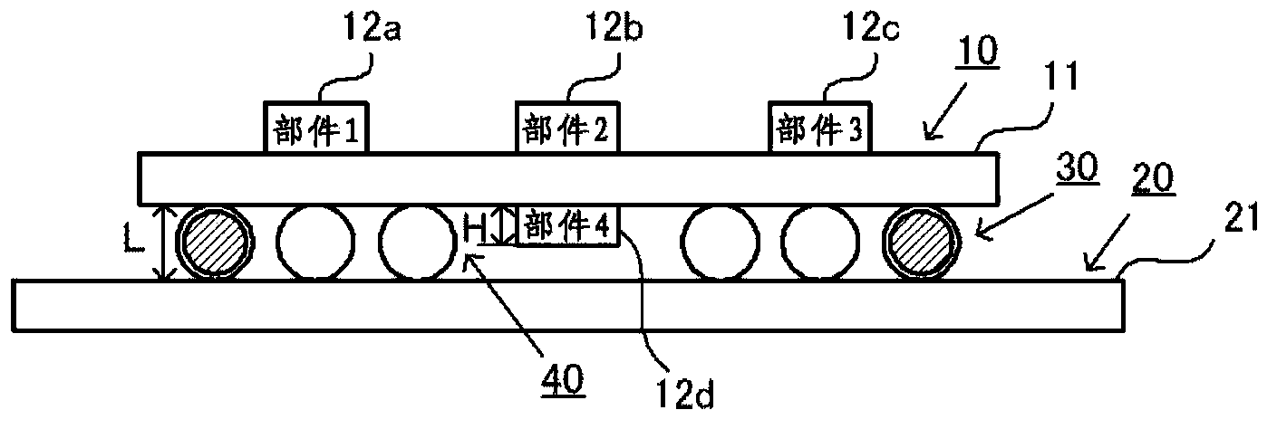
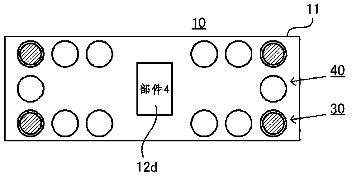
[0037] Embodiments of the present invention will be described in detail below with reference to the drawings. Figure 1A and Figure 1B It is an explanatory diagram showing the structure of a substrate device (this device) according to one embodiment of the present invention.

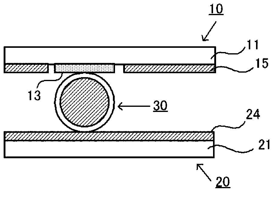
[0038] First, explain how this device works with Figure 5AThe difference between the conventional substrate devices shown by etc. In this device, a plurality of (two) substrates are mechanically and electrically connected to each other not only by resin core solder balls but also by coreless sold...


PUM


Abstract

A substrate device, includes: a plurality of substrates stacked one on another including a substrate (10) on which electronic components (12a to 12d) are mounted; and a coupling member (30 and 40) connecting mechanically and electrically the two opposed substrates (10 and 20), wherein the coupling member includes: a plurality of core-less solder balls (40) connecting mechanically and electrically the two opposed substrates (10 and 20); and a plurality of spacers (30) configured to keep a clearance between the two opposed substrates (10 and 20) wider than a mounting height of the electronic component (12d) between the substrates.

Description

[0001] Cross References to Related Applications [0002] This application claims the priority of Japanese Patent Application No. 2012-088347 submitted to the Japan Patent Office on April 09, 2012, and therefore the entire content of said Japanese Patent Application is incorporated herein by reference. technical field [0003] The present invention relates to substrate devices. Background technique [0004] In general, electronic equipment has a substrate device for downsizing the equipment and saving power. The substrate device has a plurality of substrates stacked one on top of the other, including a printed circuit board on which electronic components are mounted. In the substrate device, two opposing substrates are mechanically and electrically connected by solder balls. Thus, the mounting density of the substrate is improved. [0005] Figure 5A and Figure 5B It is a configuration explanatory diagram showing an example of a substrate device used in a conventional el...

Claims


Application Information

Patent Timeline
IPC IPC(8): H01L23/498H05K1/18
CPCH01L23/49816H01L2924/0002H01L2924/15311H01L2924/3511H01L2924/00H01L23/488
Inventor 樋渡雅哉
Owner YOKOGAWA ELECTRIC CORP
Why Eureka
Try Eureka