Electro-optic device, method for manufacturing the same, and electronic apparatus

a technology of optical devices and electronic devices, applied in the direction of semiconductor devices, diodes, electrical devices, etc., can solve the problems of difficult miniaturization of organic el elements, degradation of image quality, and inability to miniaturize organic el elements, etc., to achieve high-quality images and reduce costs

Active Publication Date: 2011-11-24
SEIKO EPSON CORP
View PDF4 Cites 40 Cited by
  • Summary
  • Abstract
  • Description
  • Claims
  • Application Information

AI Technical Summary

Benefits of technology

[0010]In the electro-optic device having such a structure, the misalignment of the color filter can be reduced. Thus, the electro-optic device can be miniaturized, and the quality of displayed images can be increased.
[0036]Thus the displaying of color images can be achieved only by adding an operation for forming color filters. Accordingly, an electro-optic device capable of displaying more high-quality images can be manufactured at a lower cost.

Problems solved by technology

In the organic EL device of JP-A-2009-146734, the bonding of the substrates is likely to cause misalignment to an extent.
This misalignment can lead to the degradation of the quality of displayed images.
Accordingly, it is difficult to miniaturize the organic EL element, or to increase the definition of the organic EL device.
Accordingly, it is difficult to form color filters having sufficient thickness, and is therefore difficult to enhance the color purity.

Method used


Image

  • Electro-optic device, method for manufacturing the same, and electronic apparatus
  • Electro-optic device, method for manufacturing the same, and electronic apparatus
  • Electro-optic device, method for manufacturing the same, and electronic apparatus

Examples


first embodiment

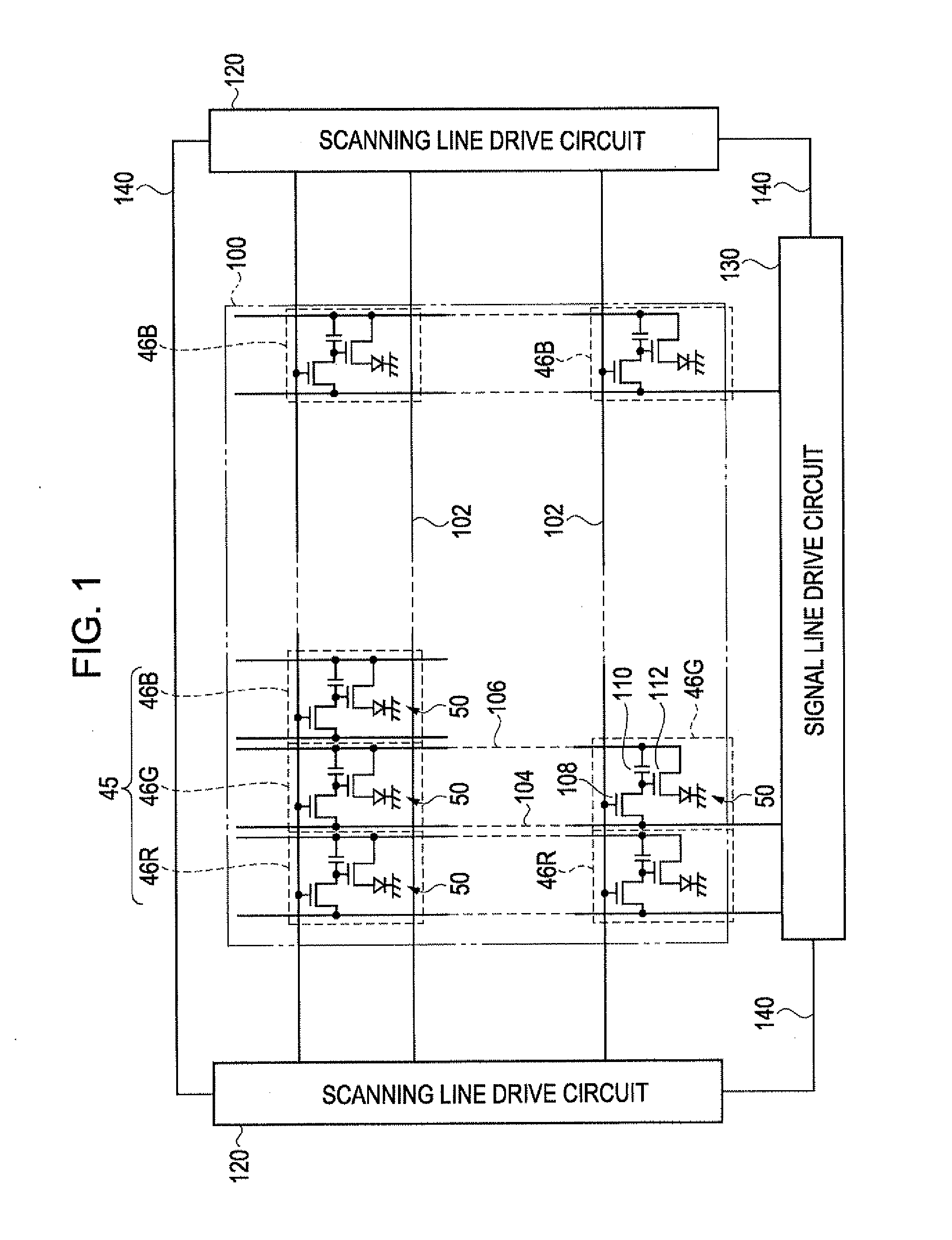
[0046]FIG. 1 is a circuit diagram of an organic EL device 1 according to a first embodiment of the invention. The organic EL device 2 according to a second embodiment of the invention has the same circuit configuration as that shown in FIG. 1. The organic EL device 1 is of an active matrix type forming color images in an image display region 100 by controlling the emission of each of organic EL elements. The image display region 100 includes a plurality of scanning lines 102, a plurality of signal lines 104 orthogonal to the scanning lines 102, and a plurality of power supply lines 106 parallel to the signal lines 104. Sub-pixels 46 are provided in the respective divisions defined by being surrounded by the three lines.

[0047]The sub-pixels 46 include red sub-pixels 46R emitting red light, green sub-pixels 46G emitting green light, and blue sub-pixels 46B emitting blue light. Each set of the three sub-pixels 46R, 46G and 46B defines a pixel 45. The color of emitted light depends on t...

second embodiment

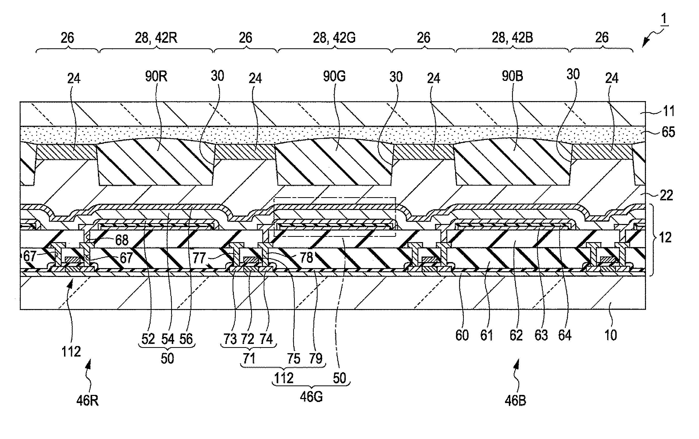
[0088]In the second embodiment, a method for manufacturing an organic EL device that is a type of electro-optic device will now be described. FIGS. 4A to 6I are sectional views illustrating the method for manufacturing an organic EL device 2 of the present embodiment. The organic EL device 2 manufacture by the method of the present embodiment is of a top emission type that can display color images and has the same structure as the organic EL device 1 of the first embodiment. The components constituting the organic EL device are the same as those in the first embodiment. The same parts are designated by the same reference numerals and the same description may be omitted.

[0089]The method of the present embodiment features the operation performed after the organic EL elements 50 (see FIG. 3) have been formed. In the present embodiment, the description of the operations up to the formation of the organic EL elements 50 is omitted. The components and elements in the element layer 12 (see...

modification 1

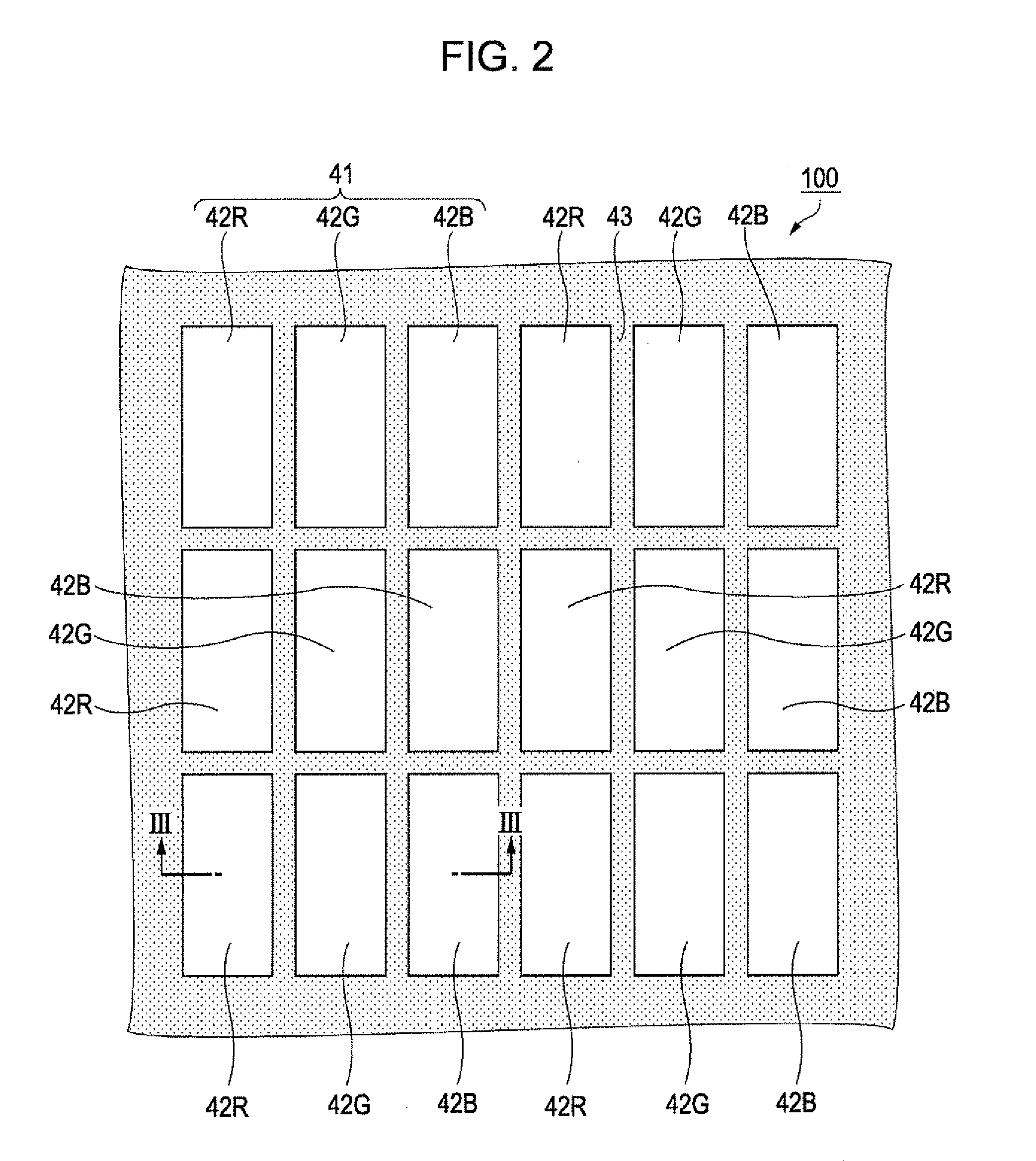
[0105]In the organic EL devices 1 and 2, each sub-pixel region 42 has a 14 μm by 4 μm rectangular shape, and the sub-pixel regions 42R, 42G and 42B are arranged in a striped manner. However, the sub-pixel regions 42 may each have an almost square shape, and may be arranged in a staggered manner.


PUM


Abstract

An electro-optic device includes a light-emitting element disposed above a substrate, an optically transparent sealing film covering the light-emitting element, and a color filter disposed on the sealing film so as to adjoin the sealing film. The sealing film includes a thin portion overlapping at least part of the light-emitting element, and a thick portion surrounding the thin portion. The thin portion and the thick portion form a recess in the sealing film. The color filter fills the recess.

Description

BACKGROUND[0001]1. Technical Field[0002]The present invention relates to an electro-optic device and a method for manufacturing the same, and to an electronic apparatus.[0003]2. Related Art[0004]As information apparatuses are diversifying, the demand for electro-optic devices capable of displaying images on a plane is increasing. Organic EL devices have been known as a type of electro-optic device, and which display images using light emitted by applying a current to an organic EL (electroluminescence) layer. In order that an organic EL device displays color images, a color filter may be used which transmits light rays having wavelengths in a specific range.[0005]For example, JP-A-2009-146734 discloses an organic EL device that includes a first substrate including organic EL elements, and a second substrate having color filters. The organic EL element includes a pair of electrodes and an organic EL layer between the electrodes, and the first and the second substrate are bonded toget...

Claims


Application Information

Patent Timeline
Patent Type & Authority Applications(United States)
IPC IPC(8): H01L51/52H01L51/56
CPCH01L27/322H01L51/5284H01L51/5253H10K59/38H10K50/865H10K50/844
Inventor IWASAKI, MASANORI
Owner SEIKO EPSON CORP
Why Eureka
Try Eureka