Epitaxial process

a technology of epitaxial layer and mos transistor, which is applied in the direction of basic electric elements, electrical apparatus, and semiconductor devices, can solve the problems of how to increase the driving current of mos transistors, which has become a critical issue, and achieves the reduction of defects such as dislocations, and easy expansion of epitaxial layer.

Active Publication Date: 2014-10-07
UNITED MICROELECTRONICS CORP
View PDF146 Cites 40 Cited by
  • Summary
  • Abstract
  • Description
  • Claims
  • Application Information

AI Technical Summary

Benefits of technology

[0008]According to the above, the present invention provides an epitaxial process, which forms a seeding layer, forms a buffer layer, performs an etching process to homogenize the buffer layer to have a flat bottom shape, and then forms an epitaxial layer on the homogenized flat bottom shape buffer layer. In this way, the homogenized flat bottom shape buffer layer is easier for the epitaxial layer to be grown thereon, and defects such as dislocations can be reduced. Moreover, the volume and the cross-sectional profile of the epitaxial layer can be adjusted by controlling the flatness and the remaining thickness of the homogenized and shaped buffer layer, thereby achieving specific electrical requirements with controlled stress caused by followed epitaxy steps. Preferably, the volume of the epitaxial layer can be enlarged by forming a thinner buffer layer through etching and shaping, thereby increasing the stresses induced by the epitaxial layer. Therefore, the stress effect induced by the epitaxial layer can be enhanced by the method of forming the homogenized flat bottom shape buffer layer of the present invention.

Problems solved by technology

As the semiconductor processes advance to very deep sub micron era such as 65-nm node or beyond, how to increase the driving current for MOS transistors has become a critical issue.
Improving the performance of an epitaxial layer to enhance the performances or achieve specific electrical requirements for formed semiconductor structure has therefore become an important issue in the industry.

Method used


Image

  • Epitaxial process
  • Epitaxial process
  • Epitaxial process

Examples


Embodiment Construction

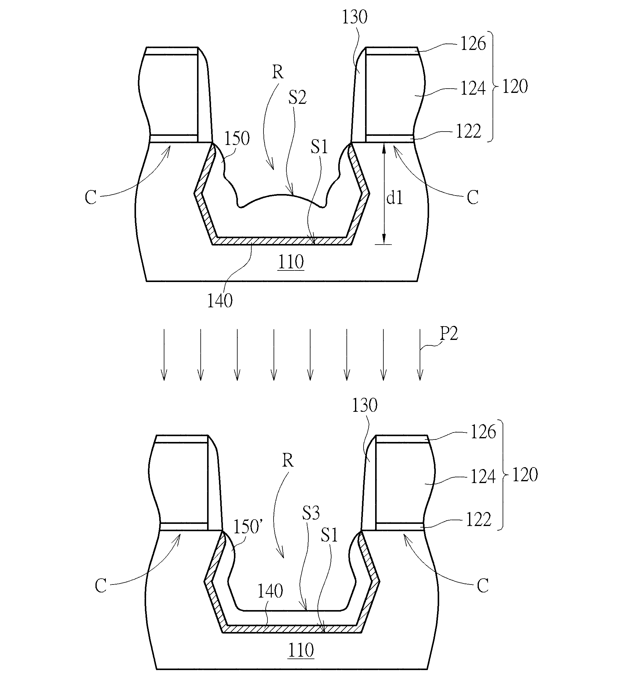
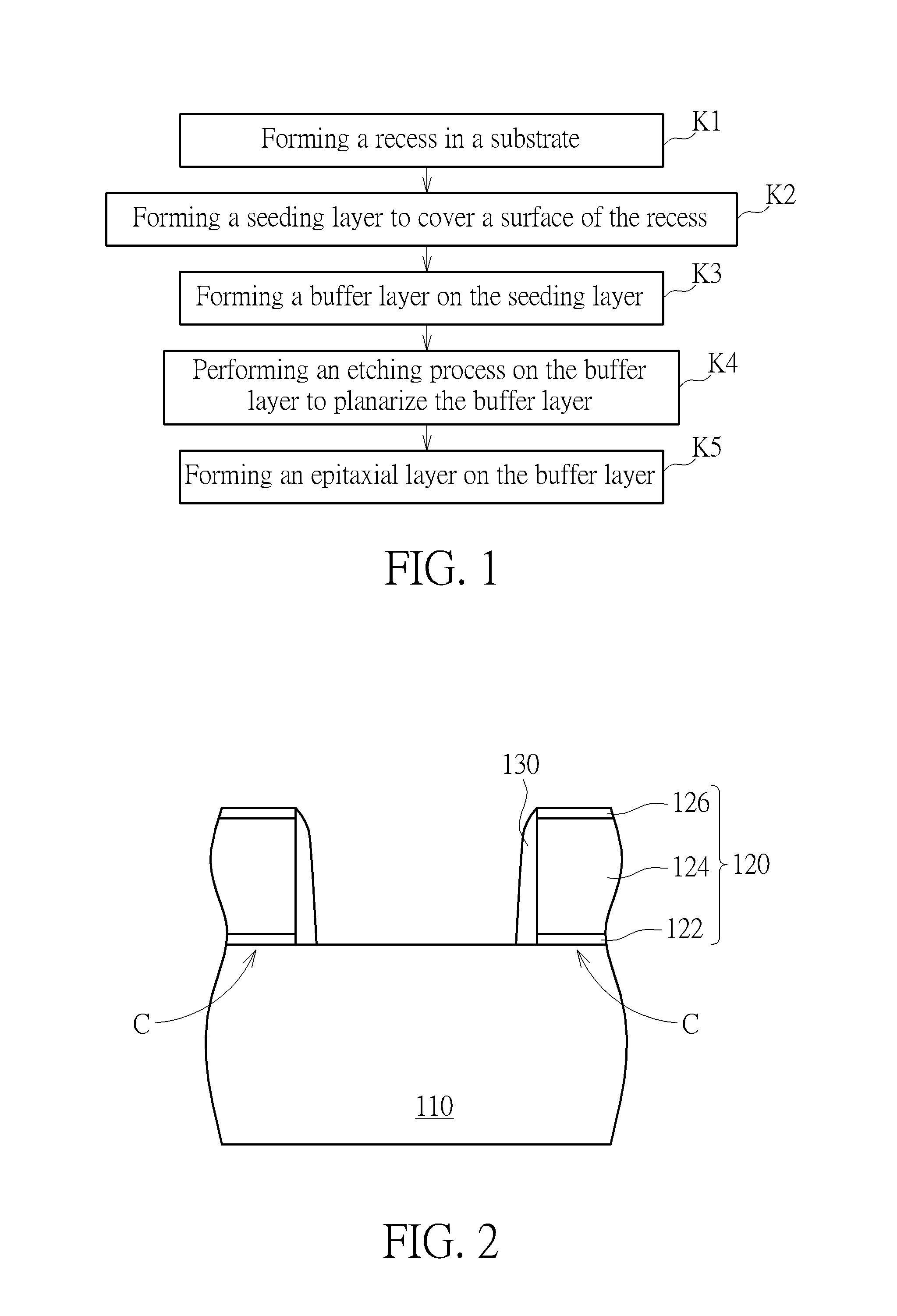
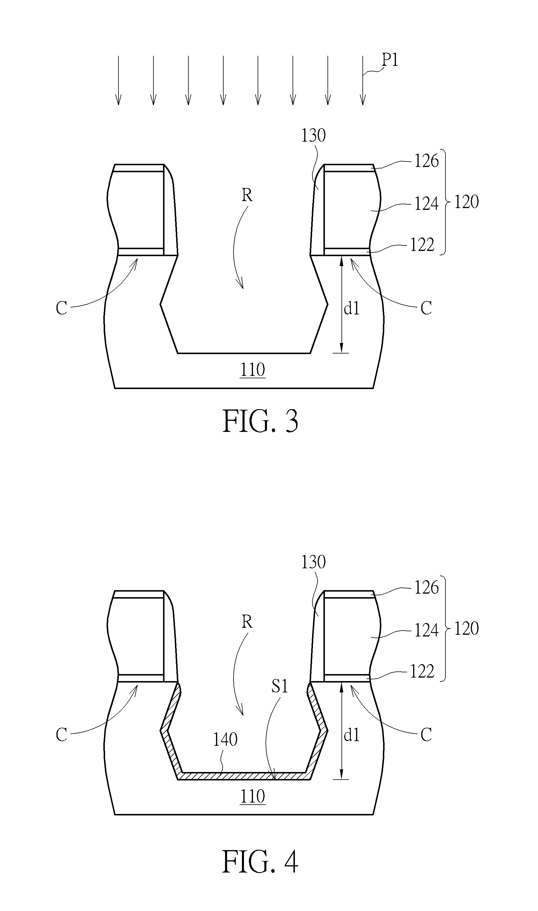
[0012]FIG. 1 schematically depicts a flow chart of an epitaxial process according to an embodiment of the present invention. FIGS. 2-8 schematically depict cross-sectional views of an epitaxial process according to an embodiment of the present invention. Two gates are depicted in this embodiment, which discloses an epitaxial process of the present invention, but the number of the gates is not restricted to it. An epitaxial layer is formed beside the gates in this embodiment, but it is not limited thereto. In this embodiment, germanium (Ge) is implanted / imported to form a silicon germanium (SiGe) layer or a silicon germanium (SiGe) epitaxial layer to form a PMOS transistor, but it is not limited thereto. In another embodiment, other elements may be implanted or imported to form the epitaxial layers; for example, P-type ions such as boron may be implanted or imported to form an epitaxial layer for forming a PMOS transistor, or carbon or N-type ions such as phosphorous may be implanted...


PUM


Abstract

An epitaxial process includes the following step. A recess is formed in a substrate. A seeding layer is formed to cover a surface of the recess. A buffer layer is formed on the seeding layer. An etching process is performed on the buffer layer to homogenize and shape the buffer layer. An epitaxial layer is formed on the homogenized flat bottom shape buffer layer.

Description

BACKGROUND OF THE INVENTION[0001]1. Field of the Invention[0002]The present invention relates generally to an epitaxial process, and more specifically to an epitaxial process, wherein a homogenized buffer layer with a flat bottom shape was formed below an epitaxial layer.[0003]2. Description of the Prior Art[0004]For decades, chip manufacturers have made metal-oxide-semiconductor (MOS) transistors faster by making them smaller. As the semiconductor processes advance to very deep sub micron era such as 65-nm node or beyond, how to increase the driving current for MOS transistors has become a critical issue. In order to improve the devices performances, crystal strain technology has been developed. Crystal strain technology is becoming more and more attractive as a means for getting better performances in the field of MOS transistor fabrication. Putting a strain on a semiconductor crystal alters the speed at which charges move through that crystal. Strain makes CMOS transistors work b...

Claims


Application Information

Patent Timeline
Patent Type & Authority Patents(United States)
IPC IPC(8): H01L21/20H01L21/02
CPCH01L21/02634H01L21/02532H01L21/0237H01L21/0245H01L21/02579H01L21/0262H01L21/02639H01L29/0847H01L29/165H01L29/66636H01L29/7848
Inventor LAI, SZU-HAOWU, CHUN-YUANCHIEN, CHIN-CHENGYU, TIEN-WEICHANG, MING-HUALIN, YU-SHUWEN, TSAI-YUHSU, HSIN-KUO
Owner UNITED MICROELECTRONICS CORP
Why Eureka
Try Eureka