Printed circuit board with long and short metal pins, and manufacture method of printed circuit board

A technology for printed circuit boards and manufacturing methods, which is applied to printed circuits, printed circuit manufacturing, printed circuit components, etc., and can solve problems such as large assembly space and difficulty in ensuring reliability

Active Publication Date: 2015-07-08
SHENZHEN SUNTAK MULTILAYER PCB
View PDF5 Cites 17 Cited by
  • Summary
  • Abstract
  • Description
  • Claims
  • Application Information

AI Technical Summary

Problems solved by technology

[0004] The purpose of the present invention is to provide a method for making a printed circuit board with long and short gold fingers, by embedding the gold fingers in the inner layer of the printed circuit board, it aims to solve the problem of the problem of the gold fingers being arranged on the printed circuit board in the prior art. The outer layer of the board causes the assembly space to be too large and it is difficult to ensure reliability

Method used


Image

  • Printed circuit board with long and short metal pins, and manufacture method of printed circuit board
  • Printed circuit board with long and short metal pins, and manufacture method of printed circuit board
  • Printed circuit board with long and short metal pins, and manufacture method of printed circuit board

Examples


Embodiment Construction

[0027] In order to make the object, technical solution and advantages of the present invention clearer, the present invention will be further described in detail below in conjunction with the accompanying drawings and embodiments. It should be understood that the specific embodiments described here are only used to explain the present invention, not to limit the present invention.

[0028] Please refer to Figure 1 to Figure 6 The method for manufacturing a printed circuit board with long and short golden fingers provided by an embodiment of the present invention includes the following steps:

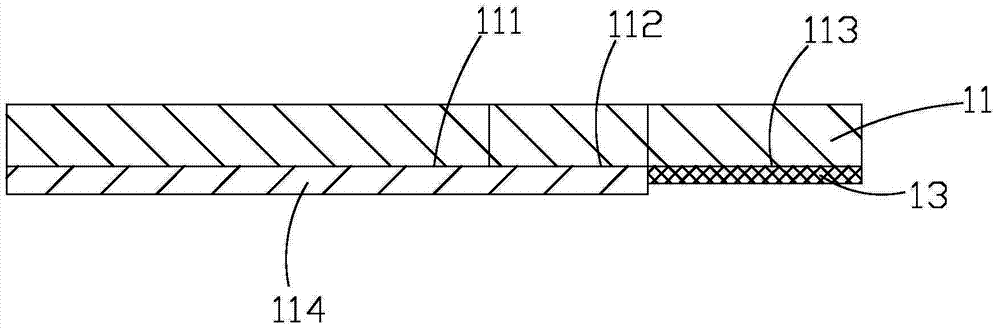
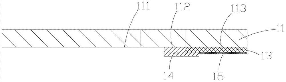
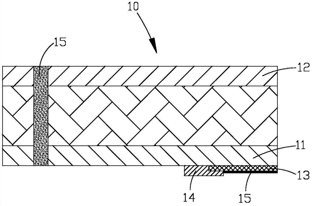
[0029] The inner layer gold finger, the step of making the inner layer gold finger includes: providing an inner layer circuit board 10, the inner layer circuit board 10 at least includes a first metal layer 11 and a second metal layer 12 facing each other. A metal layer 11 includes an inner layer circuit area 111 with a circuit pattern, an inner layer gold finger lead area 112 and an i...


PUM


Abstract

The invention is suitable for the technical field of PCB, provides a manufacture method of a printed circuit board with long and short metal pins, and aims at solving the problems that the assembling space is too large and the reliability is hard to ensure due to the fact that metal pins are arranged at the external layer of the PCB in the prior art. The manufacture method comprises the steps of preparing inner-layer metal pins, cutting an inner-layer substrate via laser, milling a prepreg, carrying out lamination and preparing outer-layer metal pins, the inner-layer metal pins are prepared on an inner-layer circuit board, the inner-layer substrate which is cut by laser is reserved, the out-layer metal pins are prepared at the surface of a first outer-layer substrate after lamination, and a second outer-layer substrate and the inner-layer substrate over the inner-layer metal are cut via a milling platform to form a step-shaped PCB embedded with the inner-layer metal pins. Thus, the quality of the embedded inner-layer metal pins is effectively protected, the assembling space of the PCB is effectively reduced, and the using reliability is ensured.

Description

technical field [0001] The invention belongs to the technical field of printed circuit boards, and in particular relates to a method for manufacturing a printed circuit board with long and short gold fingers and a printed circuit board formed by the method. Background technique [0002] In printed circuit boards, gold fingers are a common connection method. Common gold fingers include ordinary gold fingers, broken gold fingers, long and short gold fingers, etc., and these gold fingers are usually set on the outer layer of the printed circuit board. The same or similar, in order to facilitate processing. However, in the actual assembly process, the printed circuit board with such gold fingers increases the assembly space, and it is difficult to guarantee product reliability. [0003] At present, the process of making golden fingers on printed circuit boards is as follows: pre-process → copper sinking → board electrical → outer layer pattern transfer → pattern electroplating...

Claims


Application Information

Patent Timeline
Patent Type & Authority Applications(China)
IPC IPC(8): H05K3/28H05K3/46
CPCH05K1/11H05K3/281H05K3/403H05K2203/0228H05K2203/107
Inventor 何淼马江明覃红秀韩启龙赵波
Owner SHENZHEN SUNTAK MULTILAYER PCB
Why Eureka
Try Eureka