
Array substrate, display device and shutdown ghost improving circuit for display device

A power-off afterimage and display device technology is applied in the fields of array substrates, power-off afterimage improvement circuits, and display devices.

Active Publication Date: 2015-07-22
BOE TECH GRP CO LTD +1
View PDF6 Cites 47 Cited by
  • Summary
  • Abstract
  • Description
  • Claims
  • Application Information

AI Technical Summary

Problems solved by technology

[0004] Aiming at the defects in the prior art, the present invention provides a power-off afterimage improvement circuit, an array substrate, and a display device for a display device, which can solve the problem caused by the rapid drop of the high-level external bias voltage in the prior art after shutdown. charge residue problem within the pixel

Method used


Image

  • Array substrate, display device and shutdown ghost improving circuit for display device
  • Array substrate, display device and shutdown ghost improving circuit for display device
  • Array substrate, display device and shutdown ghost improving circuit for display device

Examples


Embodiment Construction

[0035] In order to make the purpose, technical solutions and advantages of the embodiments of the present invention clearer, the technical solutions in the embodiments of the present invention will be clearly and completely described below in conjunction with the drawings in the embodiments of the present invention. Obviously, the described embodiments It is a part of embodiments of the present invention, but not all embodiments. Based on the embodiments of the present invention, all other embodiments obtained by persons of ordinary skill in the art without creative efforts fall within the protection scope of the present invention.

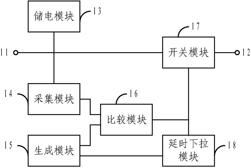
[0036] figure 1 It is a structural block diagram of a power-off afterimage improvement circuit for a display device in an embodiment of the present invention. see figure 1 , the circuit consists of:

[0037] The first connection terminal 11 and the second connection terminal 12: the first connection terminal 11 is used for connecting an externa...


PUM


Abstract

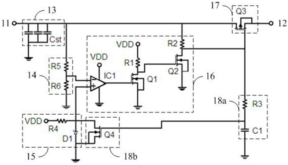
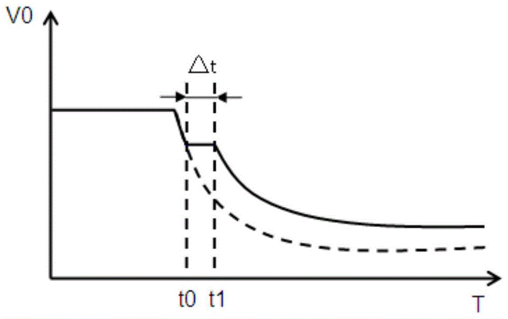
The invention provides an array substrate, a display device and a shutdown ghost improving circuit for the display device. The shutdown ghost improving circuit comprises a first connecting end, a second connecting end, an accumulation module, an acquisition module, a generation module, a comparison module, a switching module and a delay pull-down module; the first connecting end is used for being connected with external bias voltage; the second connecting end is used for being connected with a scanning driving circuit in the display device; the accumulation module is used for storing charge so as to keep potential at the first connecting end; the acquisition module is used for acquiring external bias voltage; the generation module is used for generating reference voltage with a preset initial value; the comparison module is used for generating a first control signal when sampled voltage is lower than the reference voltage; the switching module is used for cutting off electrical connection between the first connecting end and the second connecting end when receiving the first control signal; the delay pull-down module is used for pulling down the reference voltage to preset potential at preset time after the first control signal is received. The problem of charge residue in pixels due to rapid decrease of high-level external bias voltage after shutdown in the prior art can be solved.

Description

technical field [0001] The invention relates to the field of display technology, in particular to a power-off afterimage improvement circuit for a display device, an array substrate, and a display device. Background technique [0002] In TFT-LCD (Thin Film Transistor Liquid Crystal Display, thin film transistor liquid crystal display) device, XAO (Output ALL-ON Control, ie XDON or XON) is a control signal of the scan driver (Gate Driver), which is a specific The signals on all row scanning lines can be compulsorily connected to a high-level external bias voltage VGH (providing a high-level voltage for the scanning signal, that is, providing a turn-on voltage for the thin-film transistor TFT in each row of pixels). By using the XAO signal, the TFTs in all pixels can be turned on when the display device is turned off, so as to discharge the charge accumulated in each pixel, so as to prevent the afterimage after power-off. [0003] However, after the display device is turned o...

Claims


Application Information

Patent Timeline
IPC IPC(8): G09G3/36
Inventor 张媛杨炜帆霍微伟
Owner BOE TECH GRP CO LTD
Learn More