Array substrate, preparation method of array substrate, display panel and display device

A technology for array substrates and substrates, applied in optics, instruments, electrical components, etc., can solve problems such as poor light leakage in the screen, inability to cover the interval area 6, and offset in the long side direction of pixels, and achieve the effect of avoiding poor light leakage

Active Publication Date: 2015-09-02
BOE TECH GRP CO LTD +1
View PDF6 Cites 17 Cited by
  • Summary
  • Abstract
  • Description
  • Claims
  • Application Information

AI Technical Summary

Problems solved by technology

[0004] Reliability requirements for the panel include pressure test requirements, and when the panel is pressed by a large pressure, the color filter substrate 7 (CF) will be offset relative to the array substrate 8 (TFT), such as figure 1 As shown, the experiment proves that in the liquid crystal display panel of the ADS mode, the long side direction of the pixels along the ADS mode (advanced ultra-dimensional field switching mode) display panel is seriously shifted, so that the black matrix 71 (BM) cannot block the gate line 3 ( Gate line) and the common electrode line 4 (Vcom line) between the interval area 6, thus causing poor light leakage on the macro picture

Method used


Image

  • Array substrate, preparation method of array substrate, display panel and display device
  • Array substrate, preparation method of array substrate, display panel and display device
  • Array substrate, preparation method of array substrate, display panel and display device

Examples


Embodiment 1

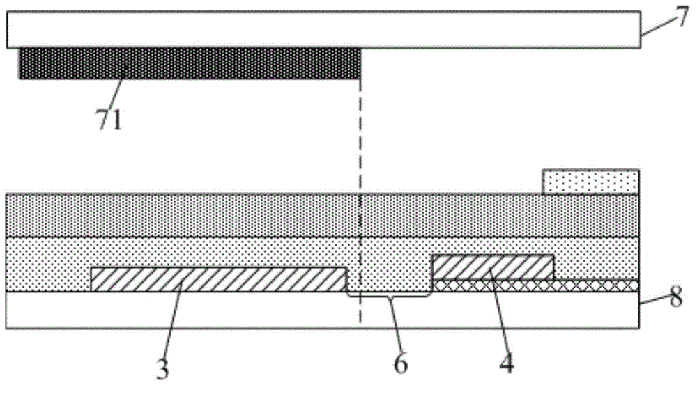
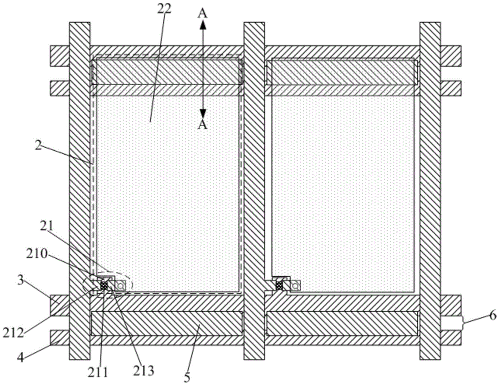
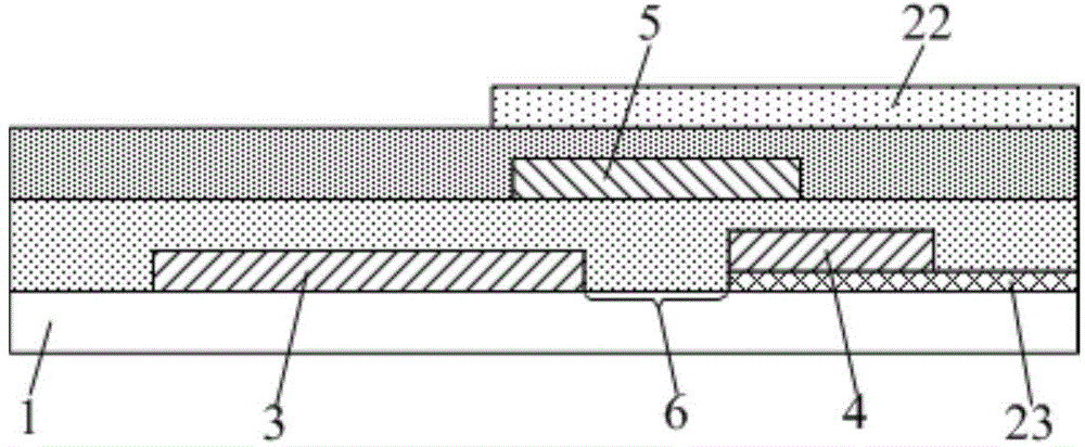
[0031] This embodiment provides an array substrate, such as figure 2 and image 3 As shown, it includes a substrate 1 and a plurality of pixel units 2 arranged in an array arranged on the substrate 1, a plurality of gate lines 3 and a plurality of common electrode lines 4, and each row of pixel units 2 corresponds to one gate line 3 and one common electrode line. The electrode lines 4, the gate lines 3 and the common electrode lines 4 corresponding to the pixel units 2 in each row are located on the same side of the pixel units 2 in each row, and are parallel to and spaced from each other, and also include a light-shielding strip 5, which is connected with the gate line 3 and the common electrode. The spacing regions 6 between the lines 4 correspond to each other, and the orthographic projection of the light-shielding strip 5 on the substrate 1 shields the spacing regions 6 .

[0032] The array substrate can shield the space region 6 between the gate line 3 and the common el...

Embodiment 2

[0046] This embodiment provides an array substrate. The difference from Embodiment 1 is that the pixel unit further includes a pixel electrode and a common electrode, the pixel electrode is arranged above the common electrode, the common electrode is arranged above the light-shielding strip, and the common electrode completely covers the light-shielding strip .

[0047] Such setting enables the common electrode to effectively shield the electric field between the light-shielding strip and the grid line and the common electrode line, so that the liquid crystal molecules correspondingly distributed in this area during display will not be disordered or the degree of disorder will be reduced. Furthermore, it is ensured that the electric field between the light-shielding strips, the grid lines and the common electrode lines will not affect the normal display.

[0048] The array substrate in this embodiment is also an array substrate in an ADS mode (Advanced Super Dimensional Field ...

Embodiment 3

[0054] This embodiment provides an array substrate. The difference from Embodiment 1-2 is that the pixel unit further includes a pixel electrode and a common electrode, the common electrode is arranged above the pixel electrode, the pixel electrode is arranged above the light-shielding strip, and the pixel electrode completely covers the Blackout strips.

[0055] Such setting also enables the pixel electrodes to effectively shield the electric field between the light-shielding strips, the gate lines and the common electrode lines, so that the liquid crystal molecules correspondingly distributed in this area will not be disordered or the degree of disordering will be reduced during display. , so as to ensure that the electric field between the light-shielding strips, the grid lines and the common electrode lines will not affect the normal display.

[0056] The array substrate in this embodiment is also an array substrate in an ADS mode (Advanced Super Dimensional Field Switchin...


PUM


Abstract

The invention provides an array substrate, a preparation method of the array substrate, a display panel and a display device. The array substrate comprises a substrate as well as multiple pixel units, multiple grid lines and multiple common electrode wires which are distributed on the substrate in an array, wherein each row of pixel units correspond to one grid line and one common electrode wire; the grid line and the common electrode wire corresponding to each row of pixel units are located on the same side of the row of pixel units and are in parallel and spaced. The array substrate further comprises light-shielding strips, wherein each light-shielding strip corresponds to a spacer region between the corresponding grid line and the corresponding common electrode wire, and the orthographic projection of each light-shielding strip shields the corresponding spacer region, so that the spacer region between each grid line and the corresponding common electrode wire cannot leak light when not shielded by black matrixes on a color film substrate, and light leakage of the array substrate is avoided.

Description

technical field [0001] The present invention relates to the field of display technology, in particular, to an array substrate and a preparation method thereof, a display panel and a display device. Background technique [0002] As thin film transistor liquid crystal display panels (TFT-LCDs) are used in more and more fields, the requirements for the reliability of the panels are also getting higher and higher. [0003] The liquid crystal panel includes a color filter substrate and an array substrate. Generally, multiple common electrode lines are provided in the array substrate, and the common electrode lines are parallel to the gate lines and distributed on the same side of each row of pixel units in a one-to-one correspondence. A spacer is provided between a common electrode line corresponding to each row of pixel units and a gate line, and the spacer can transmit light, but the spacer is usually blocked by the black matrix (BM) on the color filter substrate, so that the l...

Claims


Application Information

Patent Timeline
Patent Type & Authority Applications(China)
IPC IPC(8): G02F1/1335G02F1/1343
CPCG02F1/133512G02F1/134309G02F1/136286G02F1/1368G02F2201/121G02F2201/123G02F1/136209H01L27/14623G02F1/13439G02F1/136295
Inventor 曹雪陈希陈东薛海林谢建云王建李彦辰赵伟
Owner BOE TECH GRP CO LTD
Why Eureka
Try Eureka