Display panel

A technology for display panels and substrates, which is applied in the direction of instruments, identification devices, etc., can solve the problems of electrical performance degradation of electronic components, and achieve the effect of reducing load

Inactive Publication Date: 2015-09-02
AU OPTRONICS CORP
9 Cites 9 Cited by

AI-Extracted Technical Summary

Problems solved by technology

[0003] Since the electronic components in the display panel will generate heat during operation, once the temperature in t...

Method used

[0073] In the display panel 1 of this embodiment, the driving element 18 is disposed between the substrate 12 and the thermoelectric module 58, and the thermoelectric module 58 is disposed between the driving element 18 and the light emitting element 74. In addition, a plurality of lower electrodes 60 are disposed on the thermoelectric module 58 and respectively located in the pixel regions 14 , wherein a contact hole 56 is formed in the insulating layer 50 of each pixel region 14 , and the contact hole 56 exposes part of the driving element 18 . The lower electrodes 60 are respectively electrically connected to the driving elements 18 via the contact holes 56, and the light emitting elements 74 are respectively arranged on the lower electrodes 60 and are respectively electrically connected to the driving elements 18 via the lower electrodes 60 (or electrically connected to the lower electrodes 60 through the reflective layer 66). connection), so each driving element 18 can provide a signal to the corresponding light emitting element 74 through the lower electrode 60 . In this embodiment, the patterned dam layer 62 can be disposed on the hot end insulating substrate 54 , which can have a plurality of openings 62A respectively located in the pixel regions 14 , and the light emitting elements 74 are respectively located in the openings 62A. Moreover, at least one reflective layer 66 can be disposed on the sidewall 68 inside the opening 62A of the patterned bank layer 62 . The reflective layer 66 can reflect the light emitted from the side surface of the light-emitting element 74 toward the light-emitting surface, so as to increase the brightness of the display panel 1 . In this embodiment, a plurality of filling layers 84 are respectively filled into the openings 62A and surround the corresponding light-emitting elements 74 respectively, wherein the filling layers 84 can protect the light-emitting elements 74 and guide the light emitted by the light-emitting elements 74 G...

Abstract

The invention disclose a display panel including a substrate, a pixel array and a thermoelectric module, wherein the substrate includes a plurality of pixel areas, the pixel array being disposed on the substrate, in which the pixel array includes a plurality of drive elements and a plurality of emitting elements. The drive elements are disposed with the pixel areas, the emitting elements being disposed within the pixel areas and being respectively in electronic connection with the drive elements. The thermoelectric module being disposed within the pixel array, wherein the thermoelectric module includes a thermo-end insulation base material, a cold-end insulation base material and a plurality of thermoelectric units which are arranged between the thermo-end insulation base material and the cold-end insulation base material and are mutually in electronic connection.

Application Domain

Identification means

Technology Topic

Driven elementPixel array +2

Image

  • Display panel
  • Display panel
  • Display panel

Examples

  • Experimental program(1)

Example Embodiment

[0055] In order to enable those who are familiar with the technical field of the present invention to further understand the present invention, the preferred embodiments of the present invention are specifically listed below, and with the accompanying drawings, the composition of the present invention and the desired effects are described in detail. .
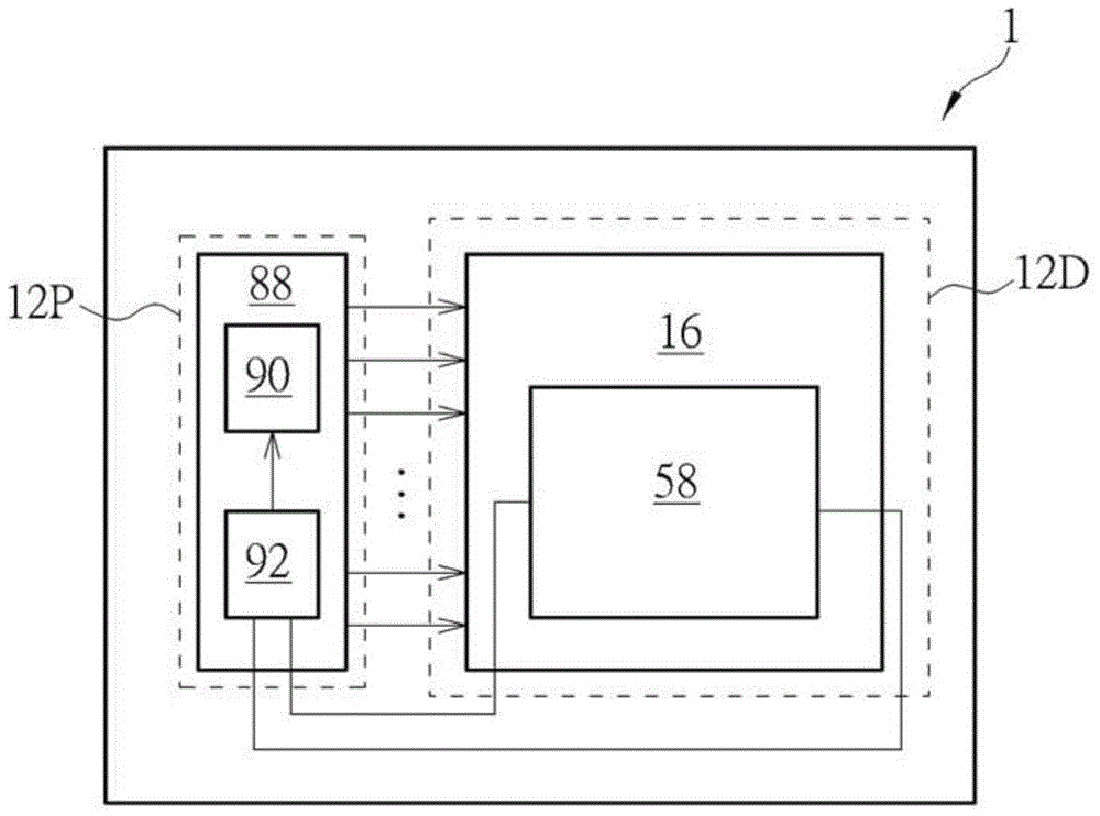
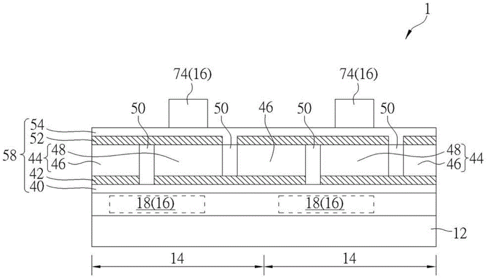
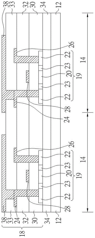
[0056] Please refer to figure 1 and figure 2. figure 1 A functional block diagram of the display panel of the present invention is shown. figure 2 A cross-sectional view of the pixel area of ​​the display panel of the present invention is shown. like figure 1 As shown, the display panel 1 of this embodiment includes a substrate 12 , a pixel array 16 , a thermoelectric module 58 and a power module 88 . The substrate 12 includes a peripheral area 12P and a display area 12D. The pixel array 16 and the thermoelectric module 58 are disposed on the display area 12D of the substrate 12 , and the power module 88 is disposed on the peripheral area 12P of the substrate 12 . The thermoelectric module 58 is electrically connected to the power module 88 , and the electric energy generated by the thermoelectric module 58 can be provided to the power module 88 . The power module 88 may include at least one main power supply 90 and one auxiliary power supply 92 , for example. The main power supply 90 may include at least one voltage converter (such as a DC-DC voltage converter) and at least one integrated circuit chip (IC chip), etc., which can transmit power or signals to various electronic components in the display panel 1 that require power or signals. . The auxiliary power supply 92 may include at least one voltage converter (such as a DC-DC voltage converter) and at least one integrated circuit chip (IC chip), etc. The auxiliary power supply 92 is electrically connected to the thermoelectric module 58, and the auxiliary power supply 92 is also connected to the main power supply 90 electrical connection. Thus, when the display panel 1 is in operation, the heat in the display panel 1 can be converted into electrical energy by the thermoelectric module 58 , and then transferred to the auxiliary power supply 92 in the power supply module 88 . Through the voltage converter and integrated circuit chip in the auxiliary power supply 92, the current generated by the thermoelectric module 58 can be boosted, bucked, negative-voltage or stabilized, so as to further transmit electric energy or signals to the main power supply 90 , or the auxiliary power supply 92 and the main power supply 90 can transmit electric energy or signals to each electronic component in the display panel 1 together. In other words, part of the electric energy required by the electronic components in the display panel 1 can be provided by the thermoelectric module 58 via the auxiliary power supply 92, so that the main power supply 90 only needs to provide the rest of the electric energy, thereby reducing the load on the main power supply 90 and reducing Display panel 1 energy consumption.
[0057] like figure 2 As shown, the display panel 1 of this embodiment has a substrate 12 , a pixel array 16 and a thermoelectric module 58 , wherein the pixel array 16 is disposed on the substrate 12 , and the thermoelectric module 58 is disposed in the pixel array 16 . The display area 12D of the substrate 12 may have a plurality of pixel areas 14 . The pixel array 16 has a plurality of driving elements 18 and a plurality of light emitting elements 74 , wherein the driving elements 18 are disposed in the pixel region 14 , and the light emitting elements 74 are disposed in the pixel region 14 and are electrically connected to the driving elements 18 respectively. In detail, the thermoelectric module 58 of this embodiment is disposed between the light emitting element 74 and the driving element 18 . The thermoelectric module 58 has a hot end insulating base material 54 , a cold end insulating base material 40 and a plurality of thermoelectric units 44 . The hot end insulating substrate 54 is disposed between the light emitting element 74 and the thermoelectric unit 44 , and the cold end insulating substrate 40 is disposed between the driving element 18 and the thermoelectric unit 44 . The thermoelectric unit 44 is disposed between the hot end insulating base material 54 and the cold end insulating base material 40 and is electrically connected to each other. Each thermoelectric unit 44 has a first channel layer 46 and a second channel layer 48 , wherein the first channel layer 46 and the second channel layer 48 have different seebeck coefficients. In this embodiment, the thermoelectric units 44 are electrically connected in series. For example, the thermoelectric module 58 may further include a plurality of first connection electrodes 52 and a plurality of second connection electrodes 42, wherein the first channel layer 46 of each thermoelectric unit 44 is connected to the The second channel layer 48 can be electrically connected with the corresponding first connection electrode 52, and the second channel layer 48 of each thermoelectric unit 44 and the first channel layer 46 of the adjacent thermoelectric unit 44 can be connected with the corresponding second connection electrode. 42 electrical connection, wherein the first connecting electrode 52 can be arranged between the thermoelectric unit 44 and the hot-end insulating substrate 54, and the second connecting electrode 42 can be arranged between the thermoelectric unit 44 and the cold-end insulating substrate 40, but not This is the limit. Thus, the thermoelectric unit 44 can form a loop, that is, a current can be formed in the thermoelectric module 58 , and if the thermoelectric module 58 is further electrically connected to a load outside the pixel array 16 , a corresponding voltage can be output. That is to say, as long as the display panel 1 is in operation, the thermoelectric module 58 can convert the heat generated by the light emitting element 74 into electric energy output, so as to achieve the effect of dissipating heat and generating additional electric energy at the same time. In other variant embodiments, the thermoelectric units 44 can also be electrically connected to each other in other ways, using an electrical connection in parallel, or a part of the thermoelectric units 44 can be electrically connected in series and another part of the thermoelectric units 44 can be electrically connected in parallel , or use other means of electrical connection. Alternatively, the thermoelectric units 44 can be divided into multiple groups, wherein the thermoelectric units 44 in each group are electrically connected to each other, while the thermoelectric units 44 in different groups are not electrically connected to each other.
[0058] Please refer to Figure 3 to Figure 13 , Figure 3 to Figure 13 A schematic diagram of a method for manufacturing a display panel according to an embodiment of the present invention is shown. like image 3 As shown, firstly, a substrate 12 is provided, and the substrate 12 includes a plurality of pixel regions 14 . The substrate 12 of this embodiment may include a rigid substrate or a flexible substrate, such as a glass substrate or a plastic substrate, but is not limited thereto. The pixel area 14 may include pixel areas for providing different colors such as red pixel area, green pixel area and blue pixel area, but not limited thereto, wherein the pixel areas 14 that can provide different colors of light are arranged in an array, by The light of different colors provided by the pixel area 14 can be mixed to achieve the effect of full-color display. Next, a plurality of driving elements 18 are formed on the substrate 12 , respectively located in the pixel area 14 . Each driving element 18 may include at least one thin film transistor, such as a silicon-based thin film transistor or an oxide semiconductor thin film transistor, and the thin film transistor may be a top gate type thin film transistor, a bottom gate type thin film transistor or other types of thin film transistors. In this embodiment, a top-gate polysilicon thin film transistor is used as the driving element 18 , which includes a semiconductor layer 19 , a gate insulating layer 30 , a gate electrode 28 , a dielectric layer 32 , a drain electrode 24 and a source electrode 26 . The semiconductor layer 19 may include, for example, a polysilicon channel layer 20. Two heavily doped semiconductor layers 22 are located on both sides of the polysilicon channel layer 20 and are respectively used as a drain doped region and a source doped region. Two lightly doped semiconductor layers 23 are respectively located Between the polysilicon channel layer 20 and the heavily doped semiconductor layer 22 . The material of the semiconductor layer 19 is not limited to polysilicon, but can be other suitable semiconductors, such as other silicon-based semiconductor layers (such as amorphous silicon, microcrystalline silicon), oxide semiconductor layers such as indium gallium zinc oxide (IGZO) or other suitable semiconductor materials. The gate insulating layer 30 covers the semiconductor layer 19 . The gate electrode 28 is located on the gate insulating layer 30 and substantially corresponds to the polysilicon channel layer 20 . The dielectric layer 32 is located on the gate electrode 28 and the gate insulating layer 30 . The drain electrode 24 and the source electrode 26 are located on the dielectric layer 32 and electrically connected to the heavily doped semiconductor layer 22 respectively. In addition, the method of this embodiment can optionally form at least one buffer layer 34 on the substrate 12 before forming the polysilicon channel layer 20, wherein the buffer layer 34 can be a single-layer structure, and the material of the buffer layer 34 can be an insulating layer such as A silicon monoxide buffer layer, a silicon nitride buffer layer, a silicon oxynitride buffer layer or an aluminum oxide buffer layer, but not limited thereto. The buffer layer 34 can also be a multi-layer structure, which can be a stack of insulating layers of different materials, such as a stack of a silicon oxide buffer layer and a silicon nitride buffer layer, but not limited thereto. In addition, the method of this embodiment can further form a protection layer 33 on the dielectric layer 32, wherein the protection layer 33 can be a single-layer structure or a multi-layer structure, and the protection layer 33 can expose part of the drain electrode 24 and the source Pole electrode 26. Next, a plurality of via electrodes 38 can be selectively formed on the protective layer 33, wherein the via electrodes 38 are respectively electrically connected to the drain electrodes 24 exposed by the protective layer 33, and the via electrodes 38 can be selected to have good electrical conductivity. Materials such as metals or alloys, but not limited thereto.
[0059] like Figure 4 As shown, a cold end insulating substrate 40 is then formed on the driving element 18 . For example, the cold end insulating base material 40 can be formed on the via electrode 38 and the protective layer 33 , but not limited thereto. The material of the insulating substrate 40 at the cold end can be an insulating material with good thermal conductivity, preferably, a ceramic material with good insulation and thermal conductivity, but not limited thereto. The cold-end insulation substrate 40 can also be a semiconductor substrate (for example, a silicon substrate) coated with silicon dioxide on the surface, or an aluminum composite substrate whose surface is anodized. like Figure 5 As shown, a plurality of second connection electrodes 42 are then formed on the cold-end insulating substrate 40, wherein there is a gap between any two adjacent second connection electrodes 42, that is, each second connection electrode 42 can be an independent The patterns are not in contact with each other. The material of the second connection electrode 42 may include materials with good electrical and thermal conductivity, preferably non-transparent conductive materials such as silver, aluminum, copper, magnesium or molybdenum, transparent conductive materials such as indium tin oxide, indium zinc oxide or oxide Aluminum zinc, a composite layer of the above materials or an alloy of the above materials, but not limited thereto.
[0060] Next, if Image 6 As shown, a plurality of thermoelectric units 44 are formed on the second connecting electrode 42 , wherein each thermoelectric unit 44 includes a first channel layer 46 and a second channel layer 48 . In detail, such as Figure 4 As shown, the first channel layer 46 and the second channel layer 48 in this embodiment can be a first semiconductor layer and a second semiconductor layer respectively. The formation method of the first semiconductor layer and the second semiconductor layer can first form a semiconductor layer on the second connection electrode 42 and the cold end insulating substrate 40, and then use a doping process (such as a diffusion process or ion implantation process) to form a semiconductor layer. process) forming a region with a first doping type and a second doping type in the semiconductor layer, and the first doping type is different from the second doping type, but not limited thereto. Then, a first semiconductor layer with a first doping type and a second semiconductor layer with a second doping type are formed by a patterning process (such as a photolithographic etching process). The first semiconductor layer and the second semiconductor layer can be a P-type semiconductor and an N-type semiconductor respectively or the first semiconductor layer and the second semiconductor layer can be an N-type semiconductor and a P-type semiconductor respectively, but not limited thereto. The substrates of the P-type semiconductor and the N-type semiconductor can be various semiconductor materials such as group IV A elements (such as silicon, germanium) and have P-type doping such as phosphorus, arsenic and N-type doping such as boron respectively. Alternatively, the substrate of P-type semiconductor and N-type semiconductor can be III-V compound semiconductor such as gallium nitride (GaN) or II-VI compound semiconductor such as zinc sulfide (ZnS), and can optionally have P-type doping Doped with N-type. In this embodiment, the first semiconductor layer and the second semiconductor layer are P-type doped silicon and N-type doped silicon respectively, but not limited thereto. It is worth mentioning that since the thermoelectric conversion efficiency of semiconductor materials is generally higher than that of metals and insulator materials, and if the combination of P-type semiconductors and N-type semiconductors can further improve the efficiency of thermoelectric conversion, the thermoelectric conversion of this embodiment The first semiconductor layer and the second semiconductor layer in the unit 44 are combined with P-type doped silicon and N-type doped silicon, which can improve the thermoelectric conversion efficiency of the overall thermoelectric unit 44 . In addition, the materials of the first channel layer 46 and the second channel layer 48 of the thermoelectric unit 44 are not limited to semiconductor materials, and metals such as antimony, copper, bismuth, nickel, cobalt or other suitable materials can also be selected.
[0061] Next, if Figure 7 As shown, an insulating layer 50 is formed between two adjacent first channel layers 46 and second channel layers 48 . In this embodiment, the first channel layer 46 , the insulating layer 50 and the second channel layer 48 are sequentially arranged along the horizontal direction, and the insulating layer 50 is located between the first channel layer 46 and the second channel layer 48 . The material of the insulating layer 50 may include inorganic materials such as silicon nitride, silicon oxide, silicon oxynitride or nitrogen-doped silicon carbide (SiCN), organic materials Such as acrylic resin (acrylic resin) or other suitable insulating materials. In this embodiment, the material of the insulating layer 50 is silicon dioxide, but not limited thereto. The method of forming the thermoelectric unit 44 and the insulating layer 50 of the present invention is not limited to the above method. For example, a plurality of disconnected insulating layers 50 may be formed first, and then the first channel layer 46 and the second channel layer 48 are respectively formed between two adjacent insulating layers 50 .
[0062] like Figure 8 As shown, a plurality of first connection electrodes 52 are then formed on the thermoelectric unit 44 . There is a gap between each adjacent first connecting electrode 52 , that is, each first connecting electrode 52 is an independent pattern and is not in contact with each other. The material of the first connection electrode 52 may include materials with good electrical and thermal conductivity, preferably non-transparent conductive materials such as silver, aluminum, copper, magnesium or molybdenum, transparent conductive materials such as indium tin oxide, indium zinc oxide or oxide Aluminum zinc, a composite layer of the above materials or an alloy of the above materials, but not limited thereto. In detail, in this embodiment, each first connection electrode 52 is electrically connected to the first channel layer 46 and the second channel layer 48 of the corresponding thermoelectric unit 44, and each second connection electrode 42 is connected to the corresponding thermoelectric unit. The second channel layer 48 of 44 is electrically connected to the first channel layer 46 of the adjacent thermoelectric unit 44 . In other words, the second channel layer 48 of each thermoelectric unit 44 is electrically connected to the first channel layer 46 of the adjacent thermoelectric unit 44, so the thermoelectric unit 44 can form a series connection through the first connection electrode 52 and the second connection electrode 42, but This is not the limit. In other variant embodiments, the thermoelectric units 44 can also be electrically connected to each other in other ways, using an electrical connection in parallel, or a part of the thermoelectric units 44 can be electrically connected in series and another part of the thermoelectric units 44 can be electrically connected in parallel .
[0063] Next, if Figure 9 As shown, the first connection electrode 52 on the corresponding part of the insulating layer 50 is formed with a patterned manufacturing process (such as a photolithographic etching process) to form an opening, wherein the opening exposes a part of the insulating layer 50 and the diameter of the opening can be r1 . Next, if Figure 10 shown. A hot end insulating substrate 54 is formed on the insulating layer 50 and the first connecting electrode 52 to form a thermoelectric module 58 . The material of the insulating base material 54 at the hot end may be an insulating material with good thermal conductivity, preferably a ceramic material with good insulation and thermal conductivity, but not limited thereto. The hot-end insulating substrate 54 can also be a semiconductor silicon substrate coated with silicon dioxide on the surface or an aluminum composite substrate with anodized surface. Subsequently, a contact hole 56 is formed in a part of the insulating base material 54 at the hot end corresponding to the opening of each first connecting electrode 52 by a patterned manufacturing process (such as a photolithographic etching process), wherein the contact hole 56 partially exposes the driving element 18, For example, the contact holes 56 partially expose the via electrodes 38 . In addition, the diameter of the contact hole 56 may be r2, and the diameter r2 of the contact hole 56 may be smaller than the diameter r1 of the opening, so that the first connection electrode 52 will not be exposed by the contact hole 56 .
[0064] like Figure 11 As shown, a plurality of lower electrodes 60 are formed on the thermoelectric module 58 and in the pixel region 14 respectively, wherein the lower electrodes 60 are respectively electrically connected to the driving element 18 through the contact hole 56, for example, the lower electrodes 60 can be connected to the driving element 18 through the transfer electrode 38. The drain electrode 24 of the element 18 is electrically connected. The material of the lower electrode 60 may preferably include a non-transparent conductive material such as silver, aluminum, copper, magnesium or molybdenum, a transparent conductive material such as indium tin oxide, indium zinc oxide or aluminum zinc oxide, a composite layer of the above materials or an alloy of the above materials, But not limited to this.
[0065] Next, if Figure 12 As shown, a patterned bank layer 62 is formed on the hot end insulating substrate 54 and the bottom electrode 60 , wherein the patterned bank layer 62 includes a plurality of openings 62A, and the openings 62A are respectively located in the pixel region 14 . In this embodiment, the material of the patterned dam layer 62 can be an organic insulating material, and preferably has photosensitivity, so that its pattern can be defined by an exposure and development process, but it is not limited thereto. The material of the patterned dam layer 62 may preferably include organic materials such as photoresist, benzocyclobutene (BCB), polymethyl methacrylate (PMMA), polyoxymethylene (POM), polybutylene terephthalate Esters (PBT), polycaprolactone (PCL), polyethylene terephthalate (PET), polycarbonate (PC), polyester (polyester), polyethylene (PE), polyphenylene ether PEEK), polylactic acid (PLA), polypropylene (PP), polystyrene (PS) or polyvinylidene chloride (PVDC), but not limited thereto. The patterned dam layer 62 can be a single-layer or multi-layer structure, and its material can also be other suitable inorganic materials, organic materials (for example, can be selected from the above-mentioned organic materials), or organic/inorganic hybrid materials. Then at least one reflective layer 66 can be selectively formed on the patterned dam layer 62, wherein the reflective layer 66 can be disposed at least on the sidewall 68 of the opening 62A of the patterned dam layer 62, and the reflective layer 66 can be further disposed on the lower The electrode 60 is on and electrically connected to the lower electrode 60 . The reflective layer 66 can be a single-layer or multi-layer structure, and its material includes reflective materials such as metals, alloys, or other suitable materials.
[0066] Next, if Figure 13As shown, a plurality of light emitting elements 74 are respectively fixed and electrically connected to each reflective layer 66 by using a plurality of conductive adhesive layers 72 . The light emitting element 74 may include an inorganic light emitting diode element, an organic light emitting diode element, or other various types of electroluminescent elements. In this embodiment, the light emitting element 74 preferably includes a plurality of inorganic light emitting diode elements, wherein each inorganic light emitting diode element includes a first electrode 78 , a second electrode 80 and a P-N diode layer 82 . The second electrode 80 is disposed on the first electrode 78 , and the P-N diode layer 82 is disposed between the first electrode 78 and the second electrode 80 . For example, in the method of this embodiment, the fabricated inorganic light emitting diode elements can be clamped or sucked by a micromechanical device, and the inorganic light emitting diode elements are respectively fixed and electrically connected to the reflective layer 66 by using the conductive adhesive layer 72 . That is to say, the conductive adhesive layer 72 is interposed between each reflective layer 66 and the first electrode 78 of each inorganic light emitting diode element. The conductive adhesive layer 72 is conductive and has a meltable property, so that the conductive adhesive layer 72 can be melted by using a thermal process. The following methods can be used for fixing the inorganic light emitting diode element. The corresponding conductive adhesive layer 72 is first formed on the reflective layer 66, and the conductive adhesive layer 72 is melted, and then the inorganic light emitting diode element is placed on the corresponding conductive adhesive layer 72 and is in contact with the conductive adhesive layer 72. After the layer 72 is cured, the inorganic light emitting diode element can be bonded and electrically connected to the reflective layer 66; or, the conductive adhesive layer 72 is first formed on the inorganic light emitting diode element, and the conductive adhesive layer 72 is melted, and then the inorganic light emitting diode element The conductive adhesive layer 72 on the light-emitting diode element is placed on the corresponding reflective layer 66 and is in contact with the reflective layer 66, and the inorganic light-emitting diode element can be bonded and electrically connected to the reflective layer 66 after the conductive adhesive layer 72 is cured. . The conductive adhesive layer 72 can be conductive glue or other suitable conductive materials, and its conductive materials can be, for example, indium (In), bismuth (Bi), tin (Sn), silver (Ag), gold, copper, gallium (Ga) and At least one of antimony (Sb), but not limited thereto. Next, a plurality of filling layers 84 are respectively filled into the openings 62A and respectively surround the corresponding light emitting elements 74 . In this embodiment, the filling layer 84 fills the spaces formed between the inorganic light emitting diode elements and the reflective layer 66 respectively. Subsequently, at least one upper electrode 86 is formed on the filling layer 84 and electrically connected to the second electrode 80 of the light-emitting element 74 to produce the display panel 1 of this embodiment, wherein the material of the upper electrode 86 can be a transparent conductive material such as oxide Indium tin, indium zinc oxide or aluminum zinc oxide, so that the light emitted by the light emitting element 74 can pass through the upper electrode 86 to provide a display effect. It is worth mentioning that the light-emitting element 74 of the present invention is not limited to using the conductive adhesive layer 72 to respectively fix and electrically connect the light-emitting element 74 to each reflective layer 66, and it can also be made by a patterned manufacturing process (such as photolithography and etching). Manufacturing process) Openings are formed in each reflective layer 66 , and then the light emitting elements 74 are respectively fixed and electrically connected to each lower electrode 60 by using the conductive adhesive layer 72 . In addition, the light emitting elements 74 of the present invention can also be formed directly on the lower electrodes 60 or the reflective layers 66 without the conductive adhesive layer 72 , but not limited thereto. In addition, in this embodiment, a light emitting element 74 is disposed in each pixel area 14 as an example for illustration, but it is not limited thereto. In other variant embodiments, a plurality of light emitting elements 74 may also be disposed in each pixel region 14 .
[0067] Please continue to refer Figure 13 , Figure 13 A schematic diagram of the display panel. like Figure 13 As shown, the structure of the display panel 1 of the present invention includes a substrate 12 , a pixel array 16 and a thermoelectric module 58 . The substrate 12 includes a plurality of pixel regions 14 . The pixel array 16 is disposed on the substrate 12 , wherein the pixel array 16 includes a plurality of driving elements 18 and a plurality of light emitting elements 74 , and the driving elements 18 and the light emitting elements 74 are disposed in the pixel area 14 . The thermoelectric module 58 is disposed in the pixel array 16 , and the thermoelectric module 58 is an element capable of driving carriers to move by using a temperature gradient or temperature difference to form a current, that is, the thermoelectric module 58 can convert heat into electrical energy. Taking this embodiment as an example, the light-emitting element 74 and the thermoelectric module 58 share the insulating substrate 54 at the hot end. When the display panel 1 is in operation, the temperature of the hot end insulating base material 54 is higher than that of the cold end insulating base material 40 located on the other side of the thermoelectric module 58, because the material of the first semiconductor layer in this embodiment is P-type doped Therefore, the majority carriers in the first semiconductor layer are holes, and the holes in the first semiconductor layer can be driven to the cold side by the temperature gradient between the hot end insulating base material 54 and the cold end insulating base material 40. The end insulating base material 40 moves. On the other hand, the material of the second semiconductor layer in this embodiment is N-type doped silicon, so the majority carriers in the second semiconductor layer are electrons, and pass through the hot end insulating base material 54 and the cold end insulating base material 40 The temperature gradient between them drives the electrons in the second semiconductor layer to move to the insulating substrate 40 at the cold end. In this way, as long as the first semiconductor layer and the second semiconductor layer in each thermoelectric unit 44 are connected in series to form a circuit through the first connection electrode 52 and the second connection electrode 42, a current can be formed in the thermoelectric module 58, and if further Connecting the thermoelectric module 58 to a load outside the pixel array 16 can output a corresponding voltage. In detail, the first semiconductor layer and the second semiconductor layer in each thermoelectric unit 44 in the thermoelectric module 58 can be connected in series to form a loop through the first connection electrode 52 and the second connection electrode 42, and the thermoelectric module 58 can be connected through the first connection electrode. 52 or the second connection electrode 42 is connected to the power module 88, but not limited thereto. In other variant embodiments, the thermoelectric units 44 can also be electrically connected to each other in other ways, using an electrical connection in parallel, or a part of the thermoelectric units 44 can be electrically connected in series and another part of the thermoelectric units 44 can be electrically connected in parallel . Specifically, in this embodiment, among the thermoelectric units 44 electrically connected to each other, the first connection electrode 52 or the second connection electrode 42 corresponding to the first channel layer 46 or the second channel layer 48 of the thermoelectric unit 44 at both terminals They can be electrically connected to the auxiliary power supply 92 in the power supply module 88 respectively through wires, and the electric energy generated by the thermoelectric unit 44 is output to the power supply module 88 , but not limited thereto. In other variant embodiments, the first connection electrodes 52 or the second connection electrodes 42 corresponding to the two first channel layers 46 or the second channel layers 48 can also be selected among the thermoelectric units 44 electrically connected to each other, and the The wires are electrically connected to an auxiliary power source 92 in the power module 88 . Alternatively, when the thermoelectric units 44 are divided into multiple groups, and the thermoelectric units 44 in different groups are not electrically connected to each other, two of the first channel layers 46 or the second channel can be selected among the thermoelectric units 44 in each group. The layer 48 corresponds to the first connection electrode 52 or the second connection electrode 42 , and is electrically connected to the auxiliary power supply 92 in the power supply module 88 through wires. Thus, as long as the display panel 1 is in operation, the thermoelectric module 58 can convert the heat generated by the light emitting element 74 into electrical energy and output it to the power module 88 to achieve the effect of dissipating heat and generating additional electrical energy.
[0068] In this embodiment, the thermoelectric module 58 includes a hot-end insulating substrate 54, a cold-end insulating substrate 40, and a plurality of thermoelectric units 44, and the thermoelectric units 44 are arranged on the hot-end insulating substrate 54 and the cold-end insulating substrate 40. between. The hot-end insulating substrate 54 is disposed between the light-emitting element 74 and the thermoelectric unit 44 , and the cold-end insulating substrate 40 is disposed between the thermoelectric unit 44 and the driving element 18 . In other words, the insulating base material 54 at the hot end is closer to the light emitting element 74 , while the insulating base material 40 at the cold end is farther away from the light emitting element 74 . Each thermoelectric unit 44 includes a first channel layer 46 and a second channel layer 48 . The material selection of the first channel layer 46 and the second channel layer 48 can be determined according to the seebeck coefficient of each material and the formula of the seebeck effect, and then according to the voltage to be generated by the thermoelectric module 58 . Table 1 lists the materials of the first channel layer 46 and the second channel layer 48 of the thermoelectric unit 44 and their Seebeck coefficients, but not limited thereto. Formula (1) is the formula of Seebeck effect where T h is the temperature of the hot end insulating base material 54, T c is the temperature of the cold end insulation base material 40, a a is the Seebeck coefficient of the first channel layer 46, a b is the Seebeck coefficient of the second channel layer 48, n is the number of thermoelectric units 44 connected in series, and ΔV ab is the voltage difference generated by the thermoelectric module 58 . For example, if the thermoelectric module 58 includes three thermoelectric units 44 connected in series, the materials of the first channel layer 46 and the second channel layer 48 of each thermoelectric unit 44 are P-type doped silicon and N-type doped silicon respectively, And the temperature difference between the two ends of the thermoelectric module 58 is 5° C. to 80° C., and the voltage difference generated by the thermoelectric module 58 may be 0.0135 volts to 0.22 volts. It is worth mentioning that the formula (1) shows that the voltage difference generated by the thermoelectric module 58 is directly proportional to the difference in the Seebeck coefficients of the materials of the first channel layer 46 and the second channel layer 48 in the thermoelectric unit 44 . That is to say, the greater the difference between the Seebeck coefficients of the materials of the first channel layer 46 and the second channel layer 48 , the higher the thermoelectric conversion efficiency of the thermoelectric module 58 will be. It can be seen from the above that if the P-type semiconductor and the N-type semiconductor are respectively used as the first channel layer 46 and the second channel layer 48 in the thermoelectric unit 44 , the thermoelectric unit 44 can provide optimal thermoelectric conversion efficiency. The material selection of the first channel layer 46 and the second channel layer 48 of the thermoelectric unit 44 is not limited to the above. The compatibility of the manufacturing process of the device is selected. In addition, the thermoelectric units 44 in the thermoelectric module 58 are not limited to be connected in series, for example, the thermoelectric units 44 may be connected in parallel or a combination of series and parallel.
[0069] Table 1
[0070]
[0071] V ab =n(a a -a b )(T h -T c )……Formula 1)
[0072] In this embodiment, the light emitting element 74 in the display panel 1 includes a plurality of inorganic light emitting diode elements, but not limited thereto. Each inorganic light emitting diode element includes a first electrode 78 , a second electrode 80 and a P-N diode layer 82 . The second electrode 80 is arranged on the first electrode 78 and the P-N diode layer 82 is arranged between the first electrode 78 and the second electrode 80, wherein the P-N diode layer 82 can be any suitable semiconductor material, which will not be repeated here. . In addition to the P-N diode layer 82 as an example, the inorganic light emitting diode element of this embodiment can also use a P-I-N (positive-intrinsic-negative) diode layer, a P-I (positive-intrinsic) diode layer, and an N-I (negative-intrinsic) diode layer. , or other suitable diode layers, or the serial connection/parallel connection of at least two kinds of diode layers mentioned above. In addition, the inorganic light-emitting diode element of this embodiment can be a miniature inorganic light-emitting diode (or called a micron-level LED, μ-LED), and its size (length and width) is substantially smaller than 5 microns, that is, the size of the inorganic light-emitting diode is Smaller than micron level, but not limited thereto. In addition, this embodiment is described as an example in which each pixel area 14 includes a light emitting element 74 , but it is not limited thereto. In other variant embodiments, a plurality of light emitting elements 74 may also be included in each pixel area 14 .
[0073]In the display panel 1 of this embodiment, the driving element 18 is disposed between the substrate 12 and the thermoelectric module 58 , and the thermoelectric module 58 is disposed between the driving element 18 and the light emitting element 74 . In addition, a plurality of lower electrodes 60 are disposed on the thermoelectric module 58 and respectively located in the pixel regions 14 , wherein a contact hole 56 is formed in the insulating layer 50 of each pixel region 14 , and the contact hole 56 exposes part of the driving element 18 . The lower electrodes 60 are respectively electrically connected to the driving elements 18 via the contact holes 56, and the light emitting elements 74 are respectively arranged on the lower electrodes 60 and are respectively electrically connected to the driving elements 18 via the lower electrodes 60 (or electrically connected to the lower electrodes 60 through the reflective layer 66). connection), so each driving element 18 can provide a signal to the corresponding light emitting element 74 through the lower electrode 60 . In this embodiment, the patterned dam layer 62 can be disposed on the hot end insulating substrate 54 , which can have a plurality of openings 62A respectively located in the pixel regions 14 , and the light emitting elements 74 are respectively located in the openings 62A. Moreover, at least one reflective layer 66 can be disposed on the sidewall 68 inside the opening 62A of the patterned bank layer 62 . The reflective layer 66 can reflect the light emitted from the side surface of the light-emitting element 74 toward the light-emitting surface, so as to increase the brightness of the display panel 1 . In this embodiment, a plurality of filling layers 84 are respectively filled into the openings 62A and surround the corresponding light-emitting elements 74 respectively, wherein the filling layers 84 can protect the light-emitting elements 74 and guide the light emitted by the light-emitting elements 74 Go in the direction of the light-emitting surface to enhance the display effect. At least one upper electrode 86 is disposed on the filling layer 84 and electrically connected to the second electrode 80 of the light emitting element 74 . In addition, the upper electrode 86 can be selectively electrically connected to a plurality of light emitting elements 74 located in different pixel regions 14 , so that the plurality of light emitting elements 74 located in different pixel regions 14 can receive a common signal.
[0074] Please refer to Figure 14 , Figure 14 A schematic cross-sectional view of a variation embodiment of the pixel region of the display panel of the present invention is shown. Different from the above-mentioned embodiments, the display panel 1 of this embodiment does not have a transfer electrode, so the lower electrodes 60 are directly electrically connected to the drain electrodes 24 exposed by the protective layer 33 through the contact holes 56, so that each driving element 18 Signals can be provided to the corresponding light emitting elements 74 through the lower electrodes 60 . Other components in the display panel of this variation embodiment can be the same as the above embodiment, and can refer to Figure 13 shown, and will not be repeated here. The manufacturing method of the display panel 1 of this embodiment is similar to the above-mentioned embodiment, except that the manufacture of the transfer electrode is omitted in the manufacturing process. Terminal insulation substrate 40. In this embodiment, the manufacturing methods of other components in the display panel are the same as those in the above embodiment, and reference may be made to Figure 3 to Figure 13 shown, so it will not be described here.
[0075] To sum up, in the display panel of the present invention, a thermoelectric module is disposed on the pixel array, and the thermoelectric module is electrically connected to the power module. That is to say, in addition to being used as a heat dissipation system for the display panel, the thermoelectric module can also be used as an auxiliary power supply system to reduce energy consumption of the display panel because it can transmit the electric energy converted by the thermoelectric module to the power module. The thermoelectric module of the present invention and the light-emitting element share the insulating base material of the hot end, so it can provide a good heat dissipation effect of the display panel. In addition, since the thermoelectric module of the present invention is arranged on the pixel array, the available thermoelectric conversion area of ​​the present invention is larger than the area of ​​the general thermoelectric module arranged in the peripheral area or other positions of the display panel, so the effect of heat dissipation and can produce The power is also more. Moreover, the thermoelectric module of the present invention is arranged on the pixel array, so the manufacturing process of the thermoelectric module can be integrated into the manufacturing process of the general display panel, without the need of additionally manufacturing the thermoelectric module, and can be manufactured with a large area of ​​the display panel.
[0076] The above descriptions are only preferred embodiments of the present invention, and all equivalent changes and modifications made according to the claims of the present invention shall fall within the scope of the present invention.

PUM

no PUM

Description & Claims & Application Information

We can also present the details of the Description, Claims and Application information to help users get a comprehensive understanding of the technical details of the patent, such as background art, summary of invention, brief description of drawings, description of embodiments, and other original content. On the other hand, users can also determine the specific scope of protection of the technology through the list of claims; as well as understand the changes in the life cycle of the technology with the presentation of the patent timeline. Login to view more.

Similar technology patents

Chromatographic analyzer

Owner:SHIMADZU CORP

Pretreatment process of organic silicon wastewater

InactiveCN102001775Areduce loadReduce effluent COD
Owner:蓝星环境工程有限公司

Portable blower

InactiveUS20050132531A1reduce loadreduce flow loss
Owner:ANDREAS STIHL AG & CO KG

Classification and recommendation of technical efficacy words

Why Eureka
Try Eureka