Electronic equipment

A technology for electronic equipment and feeding, applied in circuits, antenna equipment with additional functions, electrical components, etc., can solve problems such as affecting bandwidth and radiation efficiency, destroying product appearance design, etc., to overcome antenna bandwidth and efficiency, and maintain appearance. The effect of designing and simplifying the difficulty of debugging

Active Publication Date: 2015-09-23
HUAWEI DEVICE CO LTD
View PDF5 Cites 50 Cited by
  • Summary
  • Abstract
  • Description
  • Claims
  • Application Information

AI Technical Summary

Problems solved by technology

Furthermore, recently, electronic devices are becoming thinner and more integrated with metal element design. Traditional antenna design methods will affect bandwidth and radiation performance due to metal element shielding. Therefore, non-metallic materials must be used as antenna carriers (antenna carriers) or antenna covers in the antenna area. (antenna cover), which will damage the design of the product

Method used


Image

  • Electronic equipment
  • Electronic equipment
  • Electronic equipment

Examples


Embodiment 1

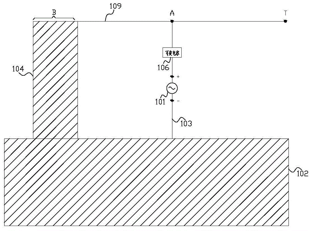
[0057] See figure 1 , figure 1It is a structural schematic diagram of the first embodiment of the electronic equipment of the present invention. Such as figure 1 As shown, the embodiment of the present invention provides an electronic device, the electronic device is provided with a metal frame, and the electronic device also includes a feed source 101, an antenna feed point+, an antenna ground 102, a feed branch 103, and a ground branch 104 , the antenna resonant arm 109, the variable capacitor 106 and the control circuit (not shown), the antenna feed point + is the positive pole of the feed source 101, the antenna resonant arm 109 is a part of the metal frame, and the antenna feed point + is located at On the feeding branch 103, the antenna resonant arm 109 is provided with a first connecting portion B and a second connecting portion A, the first connecting portion B is arranged at the first end of the antenna resonating arm 109, and the second connecting portion A is arra...

Embodiment 2

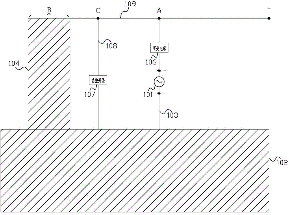
[0066] See image 3 , image 3 It is a structural schematic diagram of the second embodiment of the electronic device of the present invention. Such as image 3 As shown, the embodiment of the present invention provides an electronic device, the electronic device is provided with a metal frame, and the electronic device also includes an antenna feed point +, an antenna ground 102, a feed branch 103, a ground branch 104, and an antenna resonance Arm 109, variable capacitor 106, control circuit and short ground branch 108, antenna resonant arm 109 is a part after the metal frame is divided, antenna feed point + is located on the feed branch 103, and antenna resonant arm 109 is provided with The first connecting part B, the second connecting part A and the third connecting part C, the first connecting part B is arranged on the first end of the antenna resonating arm 109, and the second connecting part A is arranged on the first end of the antenna resonating arm 109 and the firs...

Embodiment 3

[0080] See Figure 15 , Figure 15 It is a structural schematic diagram of the third embodiment of the electronic device of the present invention. Such as Figure 15As shown, the difference between this embodiment and the second embodiment is that an inductor L1 is further provided on the basis of the second embodiment, and it is arranged in parallel with the controlled switch 107 . Specifically, when the controlled switch 107 is closed, the inductance L1 can shunt the ground current of the short ground path 108 , so as to prevent all the ground current from flowing through the controlled switch 107 and cause loss of the controlled switch 107 . In addition, when the controlled switch 107 is turned off, since the inductor L1 can also shunt the ground current of the ground path 104, the low frequency resonance can also be achieved by adjusting the inductance value of the inductor L1 when the controlled switch 107 is turned off. frequency adjustment.

[0081] For details, see...


PUM


Abstract

An electronic device is disclosed in embodiments of the present invention. The electronic device has a metal frame, and also comprises an antenna feeding point, an antenna ground, a feeding branch, a grounding branch, an antenna resonance arm, a variable capacity and a control circuit. The antenna resonance arm is a part of the partitioned metal frame, and the antenna feeding point is set on the feeding branch. A first connector and a second connector are set on the antenna resonance arm. The first connector is set on a first end of the antenna resonance arm, and the second connector is set between the first end and a second end of the antenna resonance arm. The feeding branch is set between the second connector and the antenna ground, and the grounding branch is set between the first connector and the antenna ground. The variable capacity is set on the feeding branch and between the antenna feeding point and the second connector. The control circuit is used for adjusting the capacitance of the variable capacity. According to above disclosed contents, the technical solution provided in the present invention gives attention to both the bandwidth and efficiency of the antenna, and keeps appearance uniformity of the metal frame of the whole device.

Description

technical field [0001] The invention relates to the technical field of communication, in particular to an electronic device. Background technique [0002] Today's electronic devices such as mobile phones, PDAs, and tablet computers need to increase the proportion of the display and reduce the volume of the device in order to pursue a stylish appearance, feel, and visual experience. Correspondingly, under this demand, the space that can accommodate the antenna is also increasing. smaller. [0003] In this environment, the efficiency and bandwidth of the antenna will be more difficult to achieve. Furthermore, recently, electronic devices are becoming thinner and more integrated with metal element design. Traditional antenna design methods will affect bandwidth and radiation performance due to metal element shielding. Therefore, non-metallic materials must be used as antenna carriers (antenna carriers) or antenna covers in the antenna area. (antenna cover), which will destroy...

Claims


Application Information

Patent Timeline
Patent Type & Authority Applications(China)
IPC IPC(8): H01Q1/44H01Q5/10
CPCH01Q9/42H01Q5/328H01Q5/335H01Q1/243H01Q1/48H01Q1/50
Inventor 李建铭冯堃张学飞王汉阳
Owner HUAWEI DEVICE CO LTD
Why Eureka
Try Eureka