Transparent conductive film and capacitive touch screen comprising same

A technology of transparent conductive film and transparent substrate, applied in the direction of electrical digital data processing, input/output process of data processing, instruments, etc., can solve the problems of poor adhesion of transparent conductive film, poor anti-fouling and anti-skid ability, etc., and achieve good performance , avoid pollution and reduce the effect of producing finished products

Active Publication Date: 2015-09-30
ZHANGJIAGANG KANGDE XIN OPTRONICS MATERIAL
View PDF6 Cites 2 Cited by
  • Summary
  • Abstract
  • Description
  • Claims
  • Application Information

AI Technical Summary

Problems solved by technology

[0006] The main purpose of the present invention is to provide a transparent conductive film and a capacitive touch screen containing it, to solve the problems of poor adhesion and poor anti-fouling and anti-skid ability of the transparent conductive film in the prior art

Method used


Image

  • Transparent conductive film and capacitive touch screen comprising same
  • Transparent conductive film and capacitive touch screen comprising same
  • Transparent conductive film and capacitive touch screen comprising same

Examples


Embodiment 1

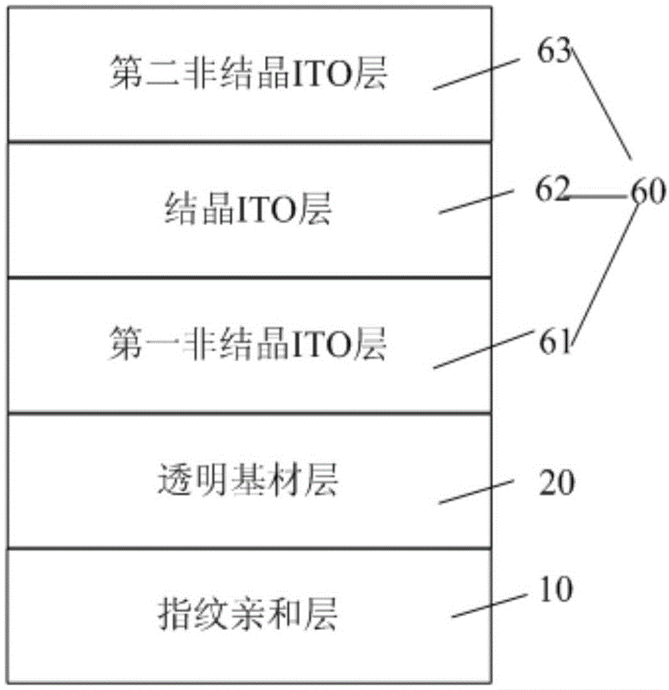
[0052] An acrylic resin layer is coated on the surface of the transparent substrate layer 20 , dried and cured to form the fingerprint affinity layer 10 .

[0053] Utilize magnetron sputtering, form the ITO layer 60 on the fingerprint affinity surface of the transparent substrate layer 20, as figure 1 As shown, the ITO layer 60 includes a first amorphous ITO layer 61 , a crystalline ITO layer 62 and a second amorphous ITO layer 63 .

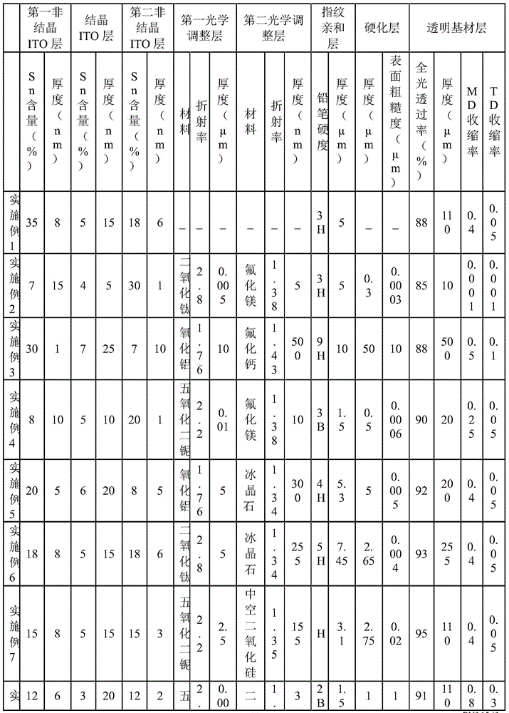
[0054] The first non-crystalline ITO layer 61, the crystalline ITO layer 62 and the second non-crystalline ITO layer 63 of the transparent conductive film are etched by an ink screen printing etching method, and then baked at a temperature of 150 ℃, the time is 60min. The specific structural parameters of the transparent conductive film are shown in Table 1.

Embodiment 2

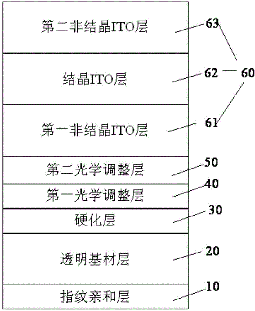
[0056]The surface of the transparent substrate layer 20 is coated with a hardening solution of the type FZ001 selected from Japan Arakawa Chemical Co., Ltd., dried and solidified to form the fingerprint affinity layer 10 . Then, in the same way, on the surface of the transparent substrate layer 20 away from the above-mentioned fingerprint affinity layer 10, a hardening solution of the type PC13-1082 selected from DIC Corporation of Japan is coated to form the hardening layer 30.

[0057] Using a magnetron sputtering process, a film is coated on the surface of the hardened layer 30 away from the above-mentioned transparent substrate layer 20, and the first optical adjustment layer 40, the second optical adjustment layer, the first amorphous ITO layer 61, and the crystalline ITO layer are sequentially obtained. layer 62 and a second amorphous ITO layer 63, forming figure 2 structure shown.

[0058] The ITO layer 60 of the transparent conductive film was etched by an ink screen...

Embodiment 3

[0060] Adopt the method identical with embodiment 1 to prepare figure 2 For the transparent conductive film shown, the structural parameters of the prepared transparent conductive film are shown in Table 1, wherein the hardening solution for coating the fingerprint affinity layer 10 is the hardening solution of FZ001 from Japan Arakawa Chemical Co., Ltd., and the coating hardening layer 30 The hardening solution used is the PC13-1082 hardening solution from DIC Corporation of Japan, and the specific structural parameters of the transparent conductive film are shown in Table 1.


PUM

PropertyMeasurementUnit
thicknessaaaaaaaaaa
thicknessaaaaaaaaaa
thicknessaaaaaaaaaa

Abstract

The invention provides a transparent conductive film and a capacitive touch screen comprising the same. The transparent conductive film comprises a fingerprint affinity layer, a transparent substrate layer and ITO (indium tin oxide) layers, wherein the transparent substrate layer is arranged on the surface of the fingerprint affinity layer; the ITO layers comprise a first amorphous ITO layer, a crystalline ITO layer and a second amorphous ITO layer; the first amorphous ITO layer is arranged on the surface, far from the fingerprint affinity layer, of the transparent substrate layer; the crystalline ITO layer is arranged on the surface, far from the transparent substrate layer, of the first amorphous ITO layer; the second amorphous ITO layer is arranged on the surface, far from the first amorphous ITO layer, of the crystalline ITO layer. The transparent conductive film has the characteristics of better adherence, better anti-pollution performance and slip resistance, lower impedance, unapparent solid lines, lower cost and simple production process.

Description

technical field [0001] The present invention relates to the field of touch screens, in particular, to a transparent conductive film and a capacitive touch screen including the same. Background technique [0002] Adhesion refers to the adhesion of two adjacent layers. The larger the adhesion, the better the adhesion. The better adhesion between each layer in the capacitive touch screen ensures the normal operation of the capacitive touch screen and ensures that the capacitive touch screen has good adhesion. If the performance and adhesion are not good, the performance of the capacitive touch screen will be affected, resulting in the peeling off of the ITO layer, poor conductivity, and even failure to work properly. Therefore, the adhesion between the layers directly affects the performance of the capacitive touch screen. In particular, the adhesion between the ITO layer and its two adjacent layers has a greater impact on the performance of the capacitive touch screen. [000...

Claims


Application Information

Patent Timeline
Patent Type & Authority Applications(China)
IPC IPC(8): G06F3/044
Inventor 徐金龙张国臻
Owner ZHANGJIAGANG KANGDE XIN OPTRONICS MATERIAL
Why Eureka
Try Eureka