Transparent conductive film and capacitive touch screen including it

A technology of capacitive touch screen and transparent conductive film, which is applied in the direction of electrical digital data processing, input/output process of data processing, instruments, etc., can solve the problem of obvious three-dimensional lines between transparent conductive film and capacitive touch screen, and achieve stress difference reduction The effect of small size, reduced production of finished products, and simple manufacturing process

Active Publication Date: 2019-03-22
ZHANGJIAGANG KANGDE XIN OPTRONICS MATERIAL
View PDF5 Cites 0 Cited by
  • Summary
  • Abstract
  • Description
  • Claims
  • Application Information

AI Technical Summary

Problems solved by technology

[0005] The main purpose of the present invention is to provide a transparent conductive film and a capacitive touch screen containing it, to solve the problem of obvious three-dimensional lines of the transparent conductive film and the capacitive touch screen in the prior art

Method used


Image

  • Transparent conductive film and capacitive touch screen including it
  • Transparent conductive film and capacitive touch screen including it
  • Transparent conductive film and capacitive touch screen including it

Examples


Embodiment 1

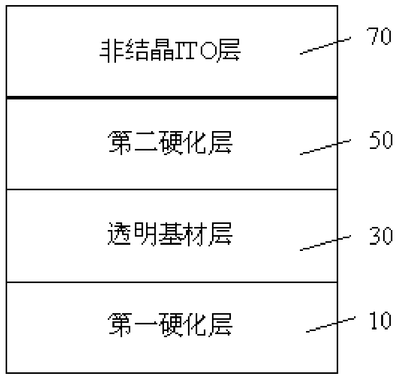
[0037] The surface of the transparent base material layer 30 is coated with a hardening solution of the type FZ001 selected from Japan Arakawa Chemical Co., Ltd., dried and cured to form the first hardened layer 10 . Then, in the same manner, the surface of the transparent substrate layer 30 far away from the first hardened layer 10 is coated with a hardening solution selected from the Japanese DIC company with a model number of PC13-1082 to form the second hardened layer 50 .

[0038] Utilize the magnetron sputtering process, on the surface of the second hardened layer 50 away from the above-mentioned transparent substrate layer 30, a film is coated to obtain an amorphous ITO layer, forming figure 1 The transparent conductive film shown.

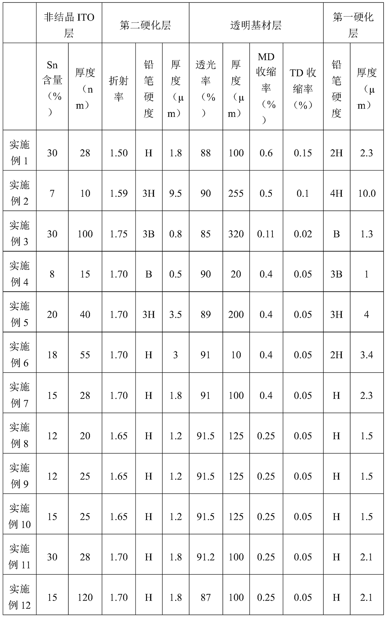
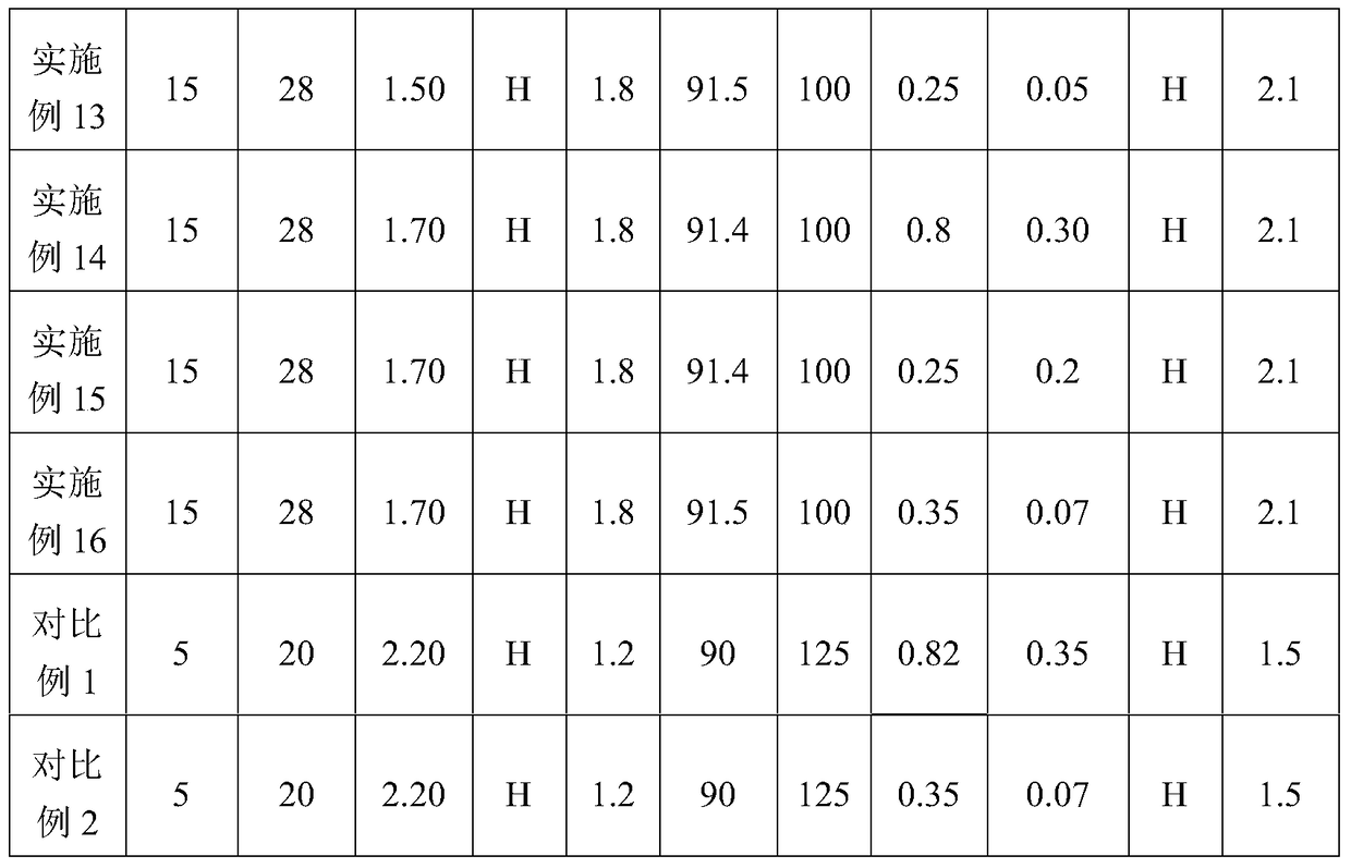
[0039] The amorphous ITO layer 70 of the transparent conductive film was etched by an ink screen printing etching method, and then baked at a temperature of 150° C. for 60 minutes. The specific structural parameters of the transparent cond...

Embodiment 2

[0041] Adopt the method identical with embodiment 1 to prepare figure 1 For the transparent conductive film shown, the structural parameters of the prepared transparent conductive film are shown in Table 1. The hardening solution for coating the first hardening layer 10 is the hardening solution of FZ001 from Japan Arakawa Chemical Co., Ltd., and the second hardening layer 50 is coated. The hardening solution is a mixed hardening solution of KZ6661 and FZ001 from JSR Corporation of Japan. The specific structural parameters of the transparent conductive film are shown in Table 1.

Embodiment 3

[0043] Adopt the method identical with embodiment 1 to prepare figure 1 For the transparent conductive film shown, the structural parameters of the prepared transparent conductive film are shown in Table 1. The hardening solution for coating the first hardening layer 10 is the hardening solution of FZ001 from Japan Arakawa Chemical Co., Ltd., and the second hardening layer 50 is coated. The hardening liquid used is the hardening liquid of the model KZ6666 of JSR Company in Japan. The specific structural parameters of the transparent conductive film are shown in Table 1.


PUM

PropertyMeasurementUnit
thicknessaaaaaaaaaa
thicknessaaaaaaaaaa
thicknessaaaaaaaaaa

Abstract

The invention provides a transparent conductive film and a capacitive touch screen comprising the same. The transparent conductive film comprises a first hardened layer, a transparent substrate layer, a second hardened layer and an amorphous ITO (indium tin oxide) layer, wherein the transparent substrate layer is arranged on the surface of the first hardened layer; the second hardened layer is arranged on the surface, far from the first hardened layer, of the transparent substrate layer; the amorphous ITO layer is arranged on the surface, far from the transparent substrate layer, of the second hardened layer. The transparent conductive film has the characteristics of low solid lines, low impedance and low cost, and a preparation process for the transparent conductive film is simpler.

Description

technical field [0001] The invention relates to the field of touch screens, in particular to a transparent conductive film and a capacitive touch screen comprising it. Background technique [0002] The existing transparent conductive film for capacitive touch screens will have three-dimensional lines after etching and heat treatment, which cannot meet the needs of some high-end customers. [0003] The main reasons for the three-dimensional pattern are: (1) The etched part of the ITO layer (indium tin oxide layer) has a difference in optical characteristics from the non-etched part (including the transmission and reflection characteristics in the visible light range, referred to as chromatic aberration), Thereby producing three-dimensional lines; (2) In the later heat treatment process, due to the difference in the thermal shrinkage rate of each layer, the stress mismatch phenomenon between the coatings will occur, which is because the ITO layer and the transparent substrate ...

Claims


Application Information

Patent Timeline
Patent Type & Authority Patents(China)
IPC IPC(8): G06F3/044
Inventor 张国臻
Owner ZHANGJIAGANG KANGDE XIN OPTRONICS MATERIAL
Why Eureka
Try Eureka