Annular PN junction

A PN junction and ring-shaped technology, applied in the direction of electrical components, circuits, semiconductor devices, etc., can solve the problems of small tolerance of constant current value and low withstand voltage

Active Publication Date: 2015-09-30
江苏东晨电子科技有限公司
View PDF4 Cites 0 Cited by
  • Summary
  • Abstract
  • Description
  • Claims
  • Application Information

AI Technical Summary

Problems solved by technology

[0004] At present, the existing constant current diode adopts J-FET technology, which is a field effect device. Its advantages ar

Method used


Image

  • Annular PN junction
  • Annular PN junction
  • Annular PN junction

Examples


Embodiment 1

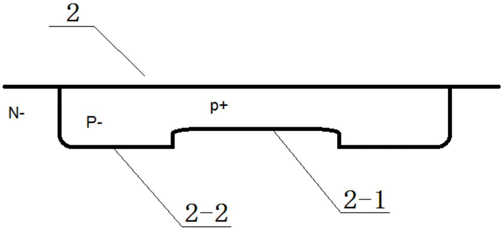
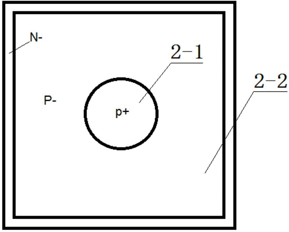
[0019] Embodiment 1, combining Figure 1-Figure 2 , a ring-shaped PN junction structure, the ring-shaped PN junction adopts a stepped PN junction 2, and a circular stepped surface depression 2-1 is constructed at the center of the PN junction surface, forming a stepped structure with the periphery 2-2.

Embodiment 2

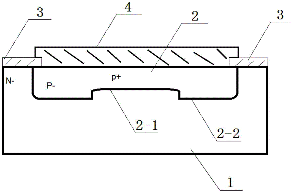
[0020] Example 2, combined with image 3 , a ring-shaped PN junction structure as described in Embodiment 1, which includes the step PN junction 2 described in Embodiment 1, the step PN junction 2 is embedded on the upper surface of the substrate 1, and the bottom of the step PN junction 2 is connected to the The upper surface of the substrate 1 is in the same plane; an oxide layer 3 is grown on the edge of the upper surface of the substrate 1, and the oxide layer 3 covers the stepped PN junction 2; an aluminum layer 4 is arranged above the bottom of the stepped PN junction 2, so Aluminum layer 4 and cover the edge of oxide layer 3 .

Embodiment 3

[0021] Embodiment 3, a ring-shaped PN junction structure as described in Embodiment 2, the substrate 1 is an N-type substrate with a thickness of 200 μm and a resistivity of 50; the thickness of the oxide layer 3 is 2 μm.


PUM

PropertyMeasurementUnit
Thicknessaaaaaaaaaa
Thicknessaaaaaaaaaa

Abstract

The invention discloses an annular PN junction. The annular PN junction adopts a step PN junction; a round step surface sunken part is formed in the center position of the PN junction surface, and a step structure is formed by the round step surface sunken part and the periphery; the annular PN junction is embedded in the upper surface of a substrate, and the bottom part of the annular PN junction and the upper surface of the substrate are positioned in the same flat surface; an oxidation layer is grown on the edge of the upper surface of the substrate, and the oxidation layer covers the annular PN junction; an aluminum layer is arranged above the bottom part of the annular PN junction, and the aluminum layer covers the edge of the oxidation layer. A constant-current diode applying the structure of the annular PN junction has a constant-current characteristic, and the breakdown voltage of the constant-current diode breaks through that of existing products by more than twice.

Description

technical field [0001] The invention relates to the field of design and manufacture of semiconductor devices, in particular to a ring-shaped PN junction. Background technique [0002] The PN junction uses different doping processes. Through diffusion, the P-type semiconductor and the N-type semiconductor are fabricated on the same semiconductor (usually silicon or germanium) substrate, and a space charge region is formed at their interface called PN. knot (English: PN junction). The PN junction has unidirectional conductivity, which is a characteristic used by many devices in electronic technology, such as the material basis of semiconductor diodes and bipolar transistors. [0003] A constant current diode is a semiconductor device that can clamp the current at a certain rated value in a fixed voltage range. It plays an important role in constant current power supplies, LED drivers and other fields. [0004] At present, the existing constant current diode adopts J-FET tech...

Claims


Application Information

Patent Timeline
IPC IPC(8): H01L29/06H01L29/861
CPCH01L29/0684H01L29/0688H01L29/861
Inventor 倪侠张俊
Owner 江苏东晨电子科技有限公司
Why Eureka
Try Eureka