Package Material For Packaging Photoelectric Device And Package

A technology for packaging materials and optoelectronic devices, applied in circuits, electrical components, semiconductor devices, etc., can solve the problems of inability to produce uniform light output, affecting the user's visual perception, poor refraction and scattering effects, etc. Save the amount of phosphor powder and improve the effect of light output

Inactive Publication Date: 2015-10-14
GENESIS PHOTONICS
View PDF0 Cites 5 Cited by
  • Summary
  • Abstract
  • Description
  • Claims
  • Application Information

AI Technical Summary

Problems solved by technology

Generally speaking, if the encapsulating gel 14 is only doped with fluorescent powder, the refraction and scattering effect on light is poor, and a uniform light output effect cannot be produced, especially in places with a large viewing angle, the uneven light color phenomenon will be more To be obvious, and thus affect the user's visual perception

Method used


Image

  • Package Material For Packaging Photoelectric Device And Package
  • Package Material For Packaging Photoelectric Device And Package
  • Package Material For Packaging Photoelectric Device And Package

Examples


Embodiment Construction

[0018] The following will clearly and completely describe the technical solutions in the embodiments of the present invention in conjunction with the accompanying drawings in the embodiments of the present invention. Obviously, the described embodiments are only some of the embodiments of the present invention, not all of them. Based on the embodiments of the present invention, all other embodiments obtained by persons of ordinary skill in the art without making creative efforts belong to the protection scope of the present invention.

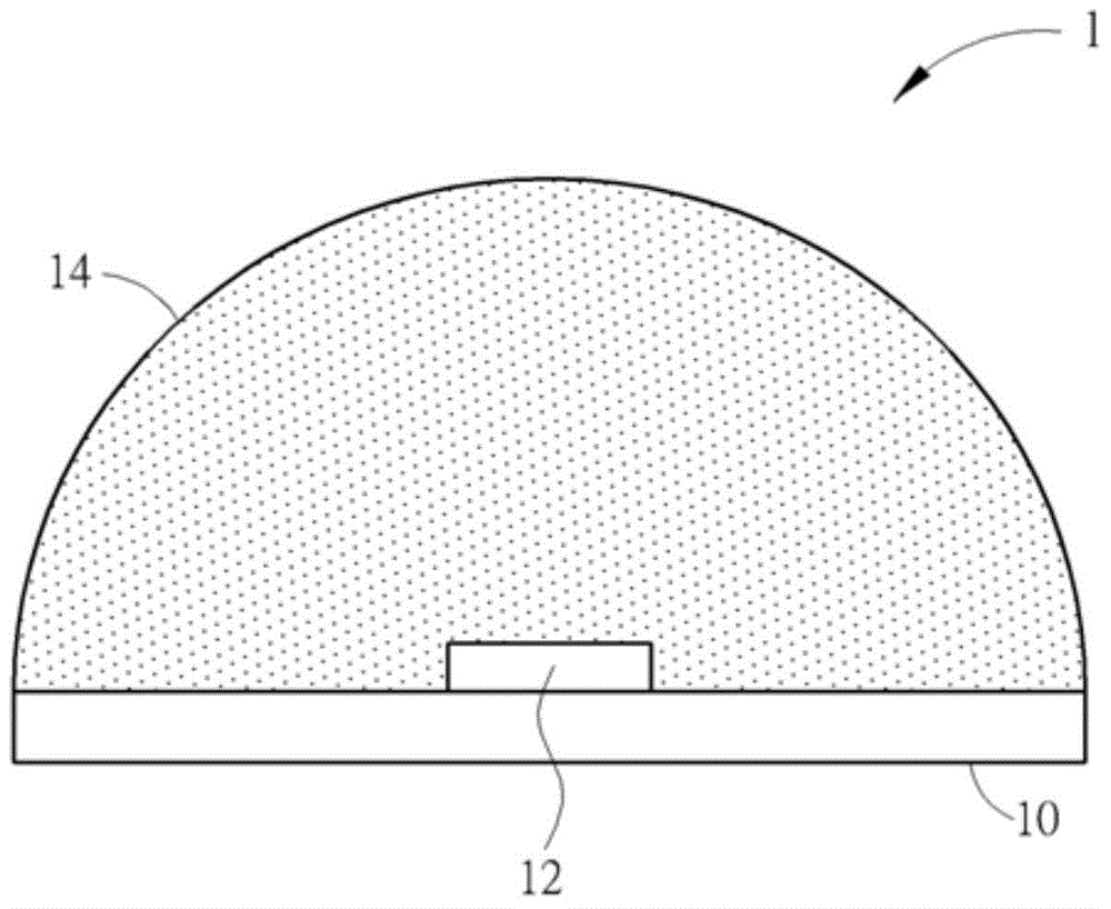
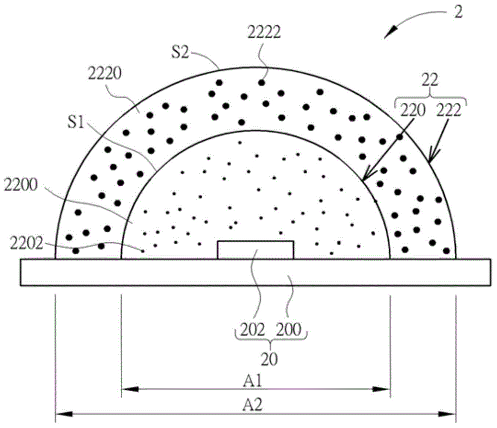
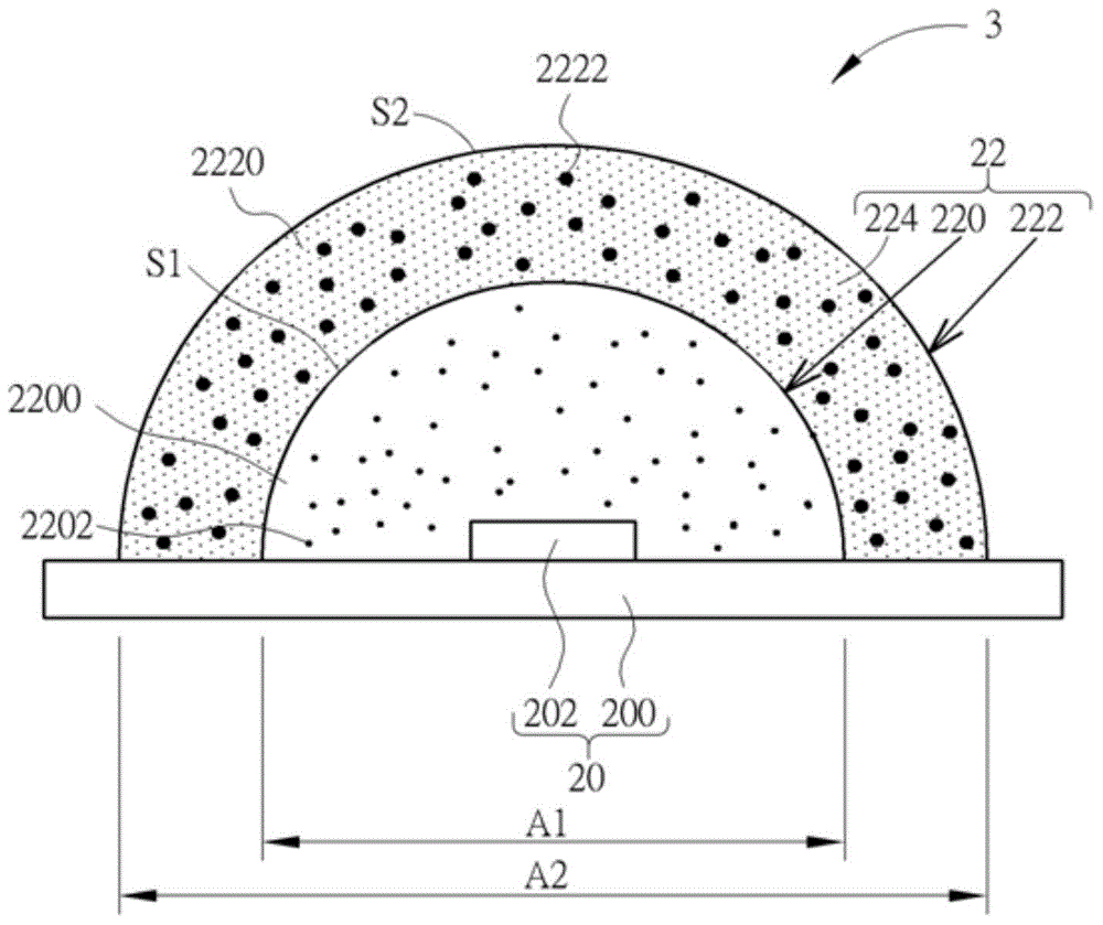
[0019] see figure 2 , figure 2 is a schematic diagram of the package structure 2 of the first embodiment of the present invention. Such as figure 2 As shown, the package structure 2 includes an optoelectronic device 20 and an encapsulation material 22 , wherein the encapsulation material 22 is used to encapsulate the optoelectronic device 20 . The photoelectric device 20 includes a bracket 200 and a light emitting diode 202 , wherein the ...


PUM

PropertyMeasurementUnit
surface roughnessaaaaaaaaaa
particle diameteraaaaaaaaaa

Abstract

A package material for packaging a photoelectric device includes a first molding portion and a second molding portion. The first molding portion is disposed on the photoelectric device. The first molding portion includes a first molding compound and a plurality of nano-scale metal oxide particles, wherein the nano-scale metal oxide particles are doped in the first molding compound. The second molding portion is disposed on the first molding portion and away from the photoelectric device. The second molding portion includes a second molding compound and a plurality of submicron-scale metal oxide particles, wherein the submicron-scale metal oxide particles are doped in the second molding compound. A whole refractive index of the first molding portion is larger than a whole refractive index of the second molding portion.

Description

technical field [0001] The invention relates to a packaging material and a packaging structure, in particular to a packaging material and a packaging structure for packaging photoelectric devices. Background technique [0002] see figure 1 , figure 1 It is a schematic diagram of a LED packaging structure 1 in the prior art. The LED packaging structure 1 includes a packaging substrate 10 , a LED chip 12 and a packaging compound 14 . The LED chip 12 is disposed on the package substrate 10 , and the encapsulant 14 is dispensed on the package substrate 10 and the LED chip 12 to package the LED chip 12 . Generally speaking, if the encapsulating gel 14 is only doped with fluorescent powder, the refraction and scattering effect on light is poor, and a uniform light output effect cannot be produced, especially in places with a large viewing angle, the uneven light color phenomenon will be more It is obvious, which in turn affects the user's visual perception. Contents of the in...

Claims


Application Information

Patent Timeline
Patent Type & Authority Applications(China)
IPC IPC(8): H01L33/56H01L33/52
CPCH01L33/58H01L33/502H01L33/54H01L33/56H01L2933/0091H01L33/507
Inventor 黄冠杰曾春铭吕文杰吴宗泽苏韦绫廖冠咏许国君
Owner GENESIS PHOTONICS
Why Eureka
Try Eureka