Fiber optic coupler array

一种光纤波导、接合部的技术,应用在波导输入和输出耦合器领域,能够解决弱偏振依赖性、集成电路制作和封装复杂、增加成本等问题

Inactive Publication Date: 2015-11-04
UNIV OF CONNECTICUT +1
View PDF15 Cites 16 Cited by
  • Summary
  • Abstract
  • Description
  • Claims
  • Application Information

AI Technical Summary

Problems solved by technology

Although lateral coupling has weak polarization dependence and is insensitive to the input bandwidth, it imposes stringent requirements on the vertical and lateral alignment of the fiber
Furthermore, SSC designs require excellent control over critical dimensions and often require lensed fibers or special fibers for nanowaveguides (especially when implemented for short wavelengths), which increases cost and complicates the fabrication and processing of integrated circuits. Complex packaging

Method used


Image

  • Fiber optic coupler array
  • Fiber optic coupler array
  • Fiber optic coupler array

Examples


Embodiment Construction

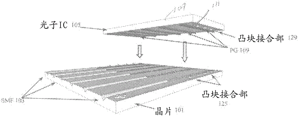
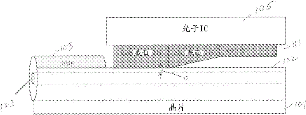
[0026] figure 1 A fiber optic coupler array 100 in accordance with the present application is illustrated. The coupler array 100 consists of two parts: a wafer 101 mechanically supporting a plurality of single-mode optical fibers (SMF) 103; and a photonic integrated circuit (IC) 105 having active electro-optical components operatively coupled to SMF 103 supported by wafer 101 . SMF 103 can extend beyond the periphery of die 101 for connection to other network components as required. Photonic IC 105 is configured in an upside-down configuration (with substrate 107 facing up), with on-chip passive semiconductor waveguide (PG) 109 being an integral part of its top surface 111 (opposite substrate 107 ). Each PG 109 is configured such that it is in intimate contact with a corresponding SMF 103 in which the fiber cross-section has been suitably modified to provide evanescent wave coupling between the SMF 103 and the PG 109 . as in image 3 and 6 As best shown in , each PG 109 c...


PUM


Abstract

An assembly includes optical fibers each having a waveguide core, a photonic integrated circuit (IC) that includes in-plane waveguides corresponding to the optical fibers, and a substrate bonded to the photonic IC with grooves that support the optical fibers. The substrate and photonic IC can have metal bumps that cooperate to provide mechanical bonding and electrical connections between the substrate and photonic IC. Portions of the optical fibers supported by the substrate grooves can define flat surfaces spaced from the optical fiber cores. The photonic IC can include passive waveguide structures with a first coupling section that interfaces to the flat surface of a corresponding optical fiber (for evanescent coupling of optical signals) and a second coupling section that interfaces to a corresponding in-plane waveguide (for adiabatic spot-size conversion of optical signals).

Description

[0001] Cross References to Related Applications [0002] This application claims priority to US Provisional Application No. 61 / 736,768, filed December 13, 2013, which is incorporated herein by reference in its entirety. technical field [0003] This application relates to waveguide input and output couplers for optical integrated circuits. Background technique [0004] Waveguide input and output couplers have always been an important issue in the design of optical integrated circuits. Various coupling schemes have been proposed or demonstrated to overcome the low coupling efficiency between optical fibers and on-chip waveguides. Based on the direction in which light is coupled into or out of the waveguide, these schemes fall into one of two categories: vertical coupling (out-of-plane) and lateral coupling (in-plane). [0005] Vertical coupling is typically accomplished with a diffraction grating incorporated into the waveguide layer to provide conversion between the single...

Claims


Application Information

Patent Timeline
Patent Type & Authority Applications(China)
IPC IPC(8): G02B6/26G02B6/42G02B6/36
CPCG02B6/305G02B6/12002G02B6/122G02B6/1228G02B6/14G02B6/421G02B6/423G02B6/4249G02B6/4257G02B2006/12038G02F1/01708G02F2001/01766
Inventor G.W.泰勒Y.张
Owner UNIV OF CONNECTICUT
Why Eureka
Try Eureka