Plasma processing apparatus

a processing apparatus and plasma technology, applied in the direction of chemical vapor deposition coating, transportation and packaging, coatings, etc., can solve the problem that the critical dimension of the bottom portion of the hole and trenches cannot be easily reached by the interface between the deposition film and the object to be processed, and the etching rate is deteriorated or the etching is stopped before it is completed, so as to improve the uniformity of both the process depth and the critical dimension across the plane of the obj

Inactive Publication Date: 2006-01-26
HITACHI HIGH-TECH CORP +1
View PDF9 Cites 121 Cited by
  • Summary
  • Abstract
  • Description
  • Claims
  • Application Information

AI Technical Summary

Benefits of technology

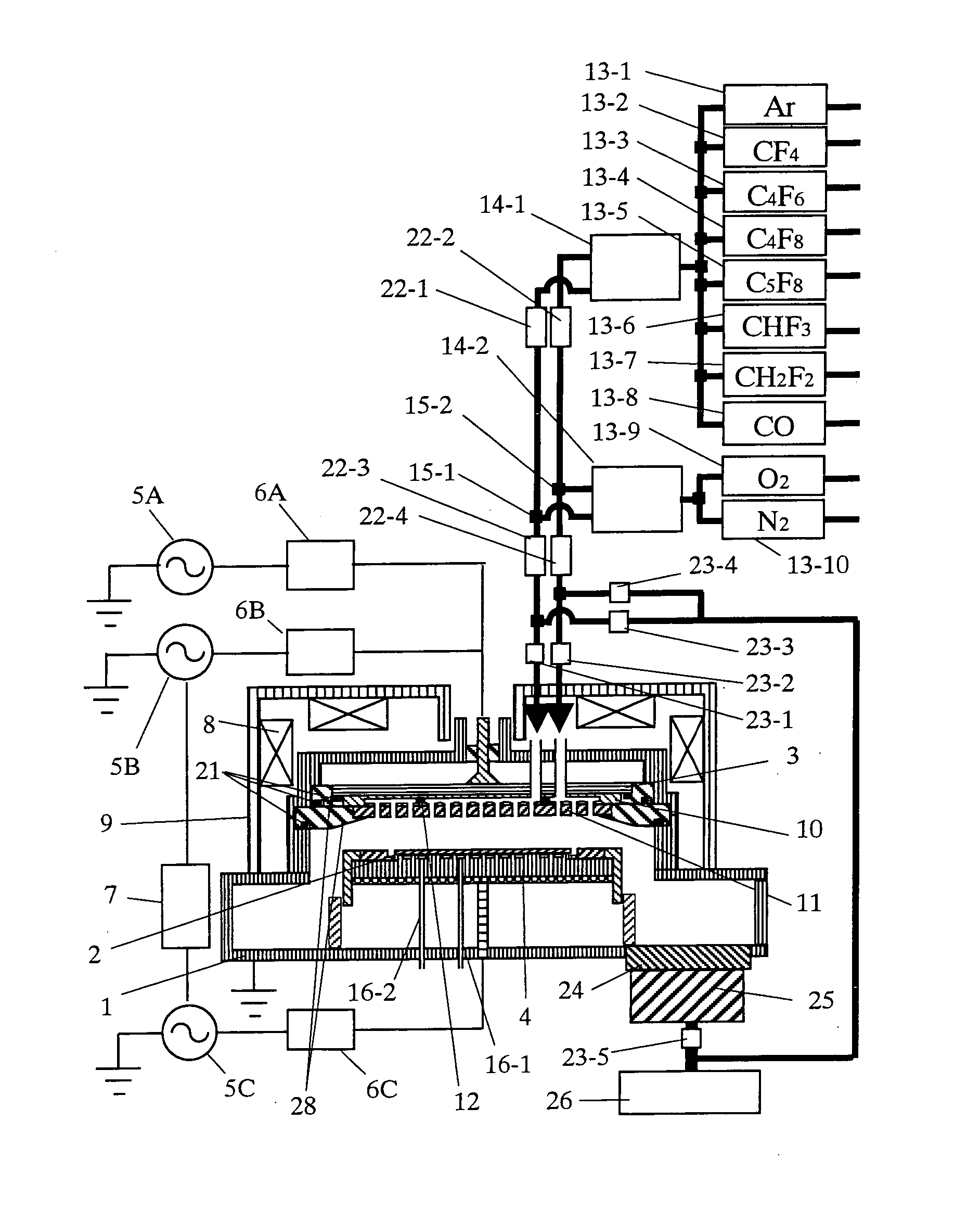
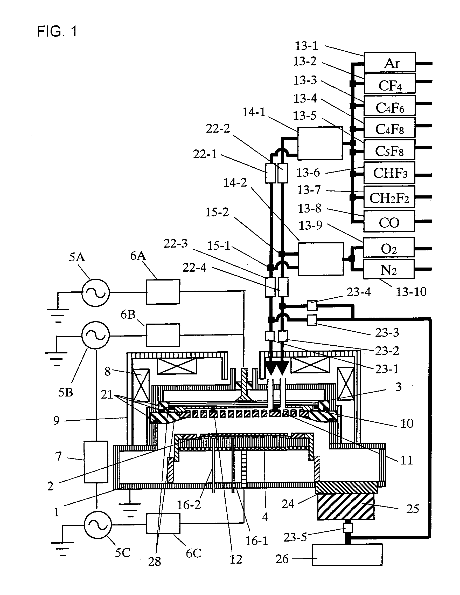
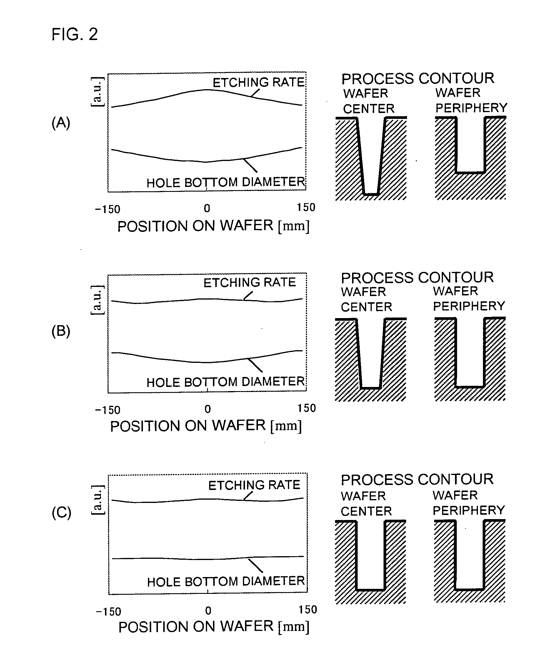
[0023] As explained, according to the present invention, at least two kinds of processing gases having different O2 or N2 composition ratios or different flow rates are introduced through different gas inlets at predetermined flow rate and composition into the processing chamber, to thereby uniformize the critical dimension across the plane of the object independently from the in-plane uniformity of the process depth. Thus, the uniformity of both the process depth and the critical dimension across the plane of the object can be improved.

Problems solved by technology

For example, according to conditions where the deposition film becomes excessively thick or conditions where considerable amount of components such as C that inhibit etching are contained in the deposition film, the etching rate is deteriorated or the etching is stopped before it is completed.
This is because the ions being incident on the object to be processed cannot easily reach the interface between the deposition film and SiOC.
Moreover, if the deposition film deposited on the side walls of the holes or trenches becomes excessively thick, the etching of the side walls of the holes and trenches may be suppressed excessively, causing the processed bottom portion of the holes and trenches to have a narrowed tapered shape.
Oppositely, if the deposition film is too thin, the lack of deposition film to be reacted with SiOC deteriorates the etching rate.
However, the process dimension regarded important in the fabrication of semiconductor devices include the process depth and the critical dimension (CD), and according to the prior art plasma processing apparatus, the in-plane uniformity of the process depth and the in-plane uniformity of the critical dimension could not be controlled independently.
Therefore, the in-plane uniformity of the critical dimension may be deteriorated by enhancing the in-plane uniformity of process depth, so it is necessary to seek the process conditions that fulfill both the in-plane uniformity of process depth and in-plane uniformity of critical dimension through trial and error, by adjusting little by little the flow rate and composition of the process gases supplied through the inner area and outer area of the shower plate, the bias power and the discharge power.

Method used


Image

  • Plasma processing apparatus
  • Plasma processing apparatus
  • Plasma processing apparatus

Examples


third embodiment

[0060]FIG. 7 is an enlarged view showing the portion where the gas dispersion plate 10 is divided into two areas, one area for dispersing the processing gas introduced through the inner gas holes into the processing chamber, and the other area for dispersing the processing gas introduced through the outer gas holes into the processing chamber. two gas dispersion plates 10-1 and 10-2; one superposed on the other, are used to disperse the processing gas. The gas dispersion plates 10-1 and 10-2 are divided into two areas, respectively, with ring-shaped partitions (for example, O-rings) 12-1 and 12-2. Moreover, the gas dispersion plates 10-1 and 10-2 are screwed using as crew 32 onto the antenna 3 via an aluminum spacer 33, for example, in order to prevent the gas dispersion plates 10-1 and 10-2 from being bent by the thickness of the O-rings. Furthermore, the gas dispersion plates 10-1 and 10-2 and the antenna 3 are separated via an insulator 31 so as to enable different RF power to b...

fourth embodiment

[0064] Next, the present invention will be described with reference to FIG. 9. According to the apparatus of the present embodiment, two RF power supplies 5A and 5C with different frequencies are connected to the electrode 4 via matching networks 6A and 6C, respectively. The present apparatus generates plasma through the RF power supplies from the RF power supplies 5A and 5C and controls the distribution of plasma by the balance of power output from the RF power supplies 5A and 5C.

[0065] In order to perform uniform etching across the plane of the object according to the present apparatus, for example, the balance between the output power of RF power supply 5A and the output power of RF power supply 5C is adjusted to control the plasma distribution and to uniformize the process depth across the plane of the object. Thereafter, by controlling the flow ratio of O2 or N2 supplied via gas outlets 36-1 and 36-2 of the top plate and through the inner gas holes and the outer gas holes of th...


PUM

PropertyMeasurementUnit
frequencyaaaaaaaaaa
frequencyaaaaaaaaaa
frequencyaaaaaaaaaa

Abstract

The object of the invention is to provide a plasma processing apparatus having enhanced plasma processing uniformity. The plasma processing apparatus comprises a processing chamber 1, means 13 and 14 for supplying processing gas into the processing chamber, evacuation means 25 and 26 for decompressing the processing chamber 1, an electrode 4 on which an object 2 to be processed such as a wafer is placed, and an electromagnetic radiation power supply 5A, wherein at least two kinds of processing gases having different composition ratios of O2 or N2 are introduced into the processing chamber through different gas inlets so as to control the in-plane uniformity of the critical dimension while maintaining the in-plane uniformity of the process depth.

Description

[0001] The present application is based on and claims priority of Japanese patent application No. 2004-217118 filed on Jul. 26, 2004, the entire contents of which are hereby incorporated by reference. FIELD OF THE INVENTION [0002] The present invention relates to a plasma processing apparatus used in the fabrication of semiconductors. DESCRIPTION OF THE RELATED ART [0003] Heretofore, plasma etching utilizing weakly-ionized plasma is adopted widely in the process of fabricating a semiconductor device such as a DRAM or a microprocessor. Now, FIG. 10 is referred to in explaining the mechanism of etching, taking the etching of an SiOC film as an example. A mixed gas containing CHF3, CF4 and N2 is used as the processing gas, for example. Radicals such as CF and CF2 dissociated from CHF3 and CF4 in the plasma are deposited on the SiOC 51 and resist 52, forming a deposition film 53. Then, the ions generated in the plasma are accelerated by bias power to be incident on the object to be proc...

Claims


Application Information

Patent Timeline
Patent Type & Authority Applications(United States)
IPC IPC(8): C23F1/00
CPCH01J37/32082H01J37/3244H01L21/3065H01J37/32449C23C16/505C23C16/509C23C16/50C23C16/455C23C16/503Y10T137/0402
Inventor KOBAYASHI, HIROYUKIMAEDA, KENJIYOKOGAWA, KENETSUIZAWA, MASARUKANEKIYO, TADAMITSU
Owner HITACHI HIGH-TECH CORP
Why Eureka
Try Eureka