Array substrate and liquid-crystal display panel

A liquid crystal display panel and array substrate technology, which is applied in nonlinear optics, instruments, optics, etc., can solve the problems of uneven surface and dark lines on the array substrate, achieve surface smoothness, reduce dark lines, and avoid overlapping Effect

Active Publication Date: 2015-11-25
TCL CHINA STAR OPTOELECTRONICS TECH CO LTD
View PDF7 Cites 17 Cited by
  • Summary
  • Abstract
  • Description
  • Claims
  • Application Information

AI Technical Summary

Problems solved by technology

[0005] The purpose of the present invention is to provide an array substrate and a liquid crystal display panel to solve the technical problem in the prior art that the surface of the array substrate side is uneven and dark lines are prone to appear due to overlap between adjacent color filters and color resists.

Method used


Image

  • Array substrate and liquid-crystal display panel
  • Array substrate and liquid-crystal display panel
  • Array substrate and liquid-crystal display panel

Examples


Embodiment Construction

[0037] The following descriptions of the various embodiments refer to the accompanying drawings to illustrate specific embodiments in which the present invention can be practiced. The directional terms mentioned in the present invention, such as "up", "down", "front", "back", "left", "right", "inside", "outside", "side", etc., are for reference only The orientation of the attached schema. Therefore, the directional terms used are used to illustrate and understand the present invention, but not to limit the present invention. In the figures, structurally similar units are denoted by the same reference numerals.

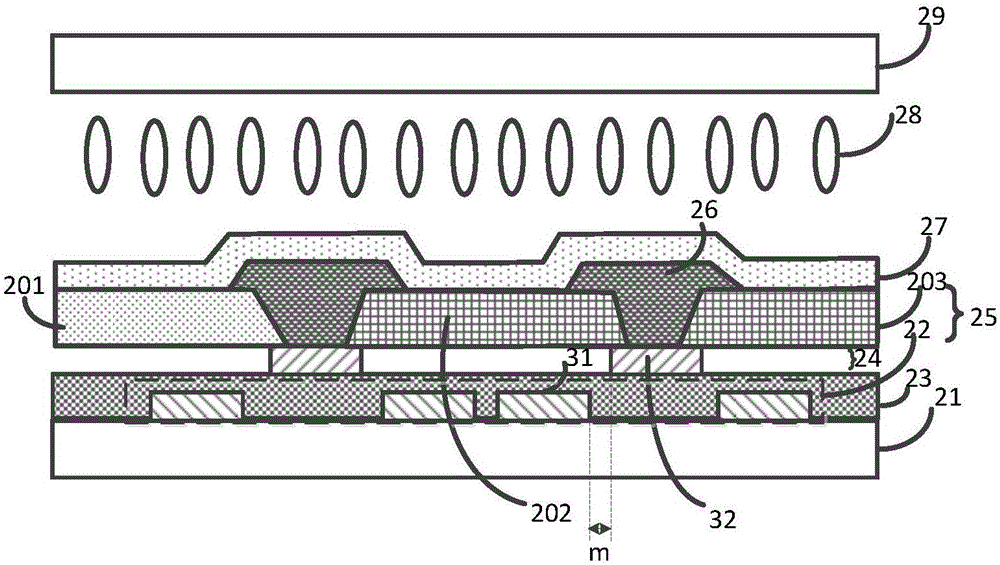
[0038] Please refer to image 3 , image 3 It is a structural schematic diagram of the first liquid crystal display panel of the present invention.

[0039] The array substrate of the present invention includes: a first substrate, such as a BOA (BMonArray) substrate, which includes a base substrate 21, a first metal layer 24, a color resist layer 25, a black matrix...


PUM


Abstract

The invention provides an array substrate and a liquid-crystal display panel, wherein the array substrate comprises an underlayer substrate, a first metal layer, a color resistance layer, a black matrix layer and a transparent conductive layer; the color resistance layer comprises a plurality of colorful film color resistances; two adjacent colorful film color resistances are set at interval. By adopting the array substrate and the liquid-crystal display panel provided herein, the colorful film color resistances are set at interval, thus avoiding overlapping between the colorful film color resistances; further the surface of the array substrate is flattened; and dark fringe is reduced.

Description

【Technical field】 [0001] The invention relates to the technical field of liquid crystal displays, in particular to an array substrate and a liquid crystal display panel. 【Background technique】 [0002] Existing liquid crystal display panel comprises: first substrate, second substrate 19, and first substrate is for example BOA (BMonArray) substrate, and BOA substrate is to make color filter film and black matrix on array substrate; It comprises base substrate 11 , shielding metal wire 12, insulating layer 13 between the shielding metal wire 12 and the data line; data line 14, color resistance layer 15, black matrix layer 16, transparent conductive layer 17, liquid crystal layer 18; color resistance layer 15 includes red Color film 101, green color film 102, blue color film 103. In order to reduce the coupling capacitance between the data line and the transparent conductive layer, the liquid crystal display adds a shielding metal line 12 on both sides of the data line 14 to p...

Claims


Application Information

Patent Timeline
Patent Type & Authority Applications(China)
IPC IPC(8): G02F1/1335G02F1/1362
CPCG02F1/133512G02F1/133514G02F1/136209G02F1/136222
Inventor 叶成亮付如海邱杰张君恺林永伦
Owner TCL CHINA STAR OPTOELECTRONICS TECH CO LTD
Why Eureka
Try Eureka