TFT array substrate structure and manufacturing method thereof

An array substrate structure, horizontal direction technology, applied in nonlinear optics, instrumentation, optics, etc., can solve the problem that the driving ability of the common electrode is not enough to meet the uniformity of the common voltage, so as to improve the display quality of the screen, improve the uniformity, and distribute uniform effect

Active Publication Date: 2015-11-25
TCL CHINA STAR OPTOELECTRONICS TECH CO LTD
View PDF7 Cites 22 Cited by
  • Summary
  • Abstract
  • Description
  • Claims
  • Application Information

AI Technical Summary

Problems solved by technology

[0005] Traditional TFT array substrates generally only have horizontal common electrode lines used to connect a row of common electrodes. For large-size and high-resolution liquid crystal display panels, only horizontal common electrode lines are provided so that the driving capability of the common electrodes is not enough to meet the uniformity of the common voltage. sexual needs

Method used


Image

  • TFT array substrate structure and manufacturing method thereof
  • TFT array substrate structure and manufacturing method thereof
  • TFT array substrate structure and manufacturing method thereof

Examples


Embodiment Construction

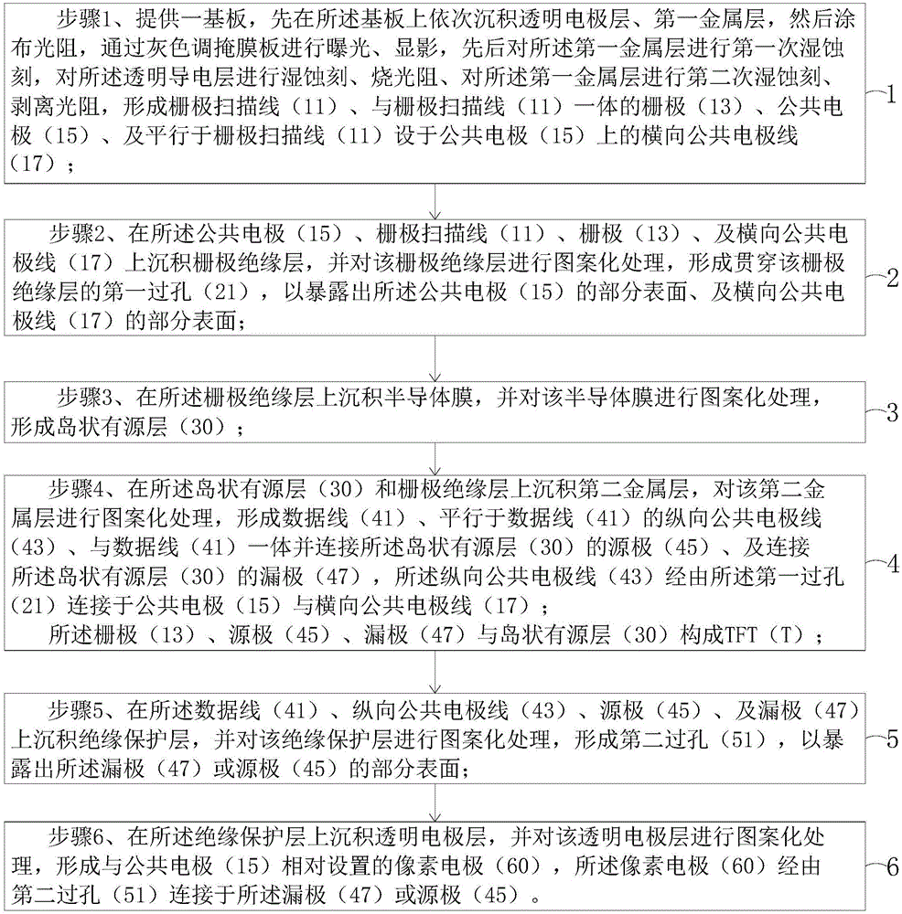
[0052] In order to further illustrate the technical means adopted by the present invention and its effects, the following describes in detail in conjunction with preferred embodiments of the present invention and accompanying drawings.

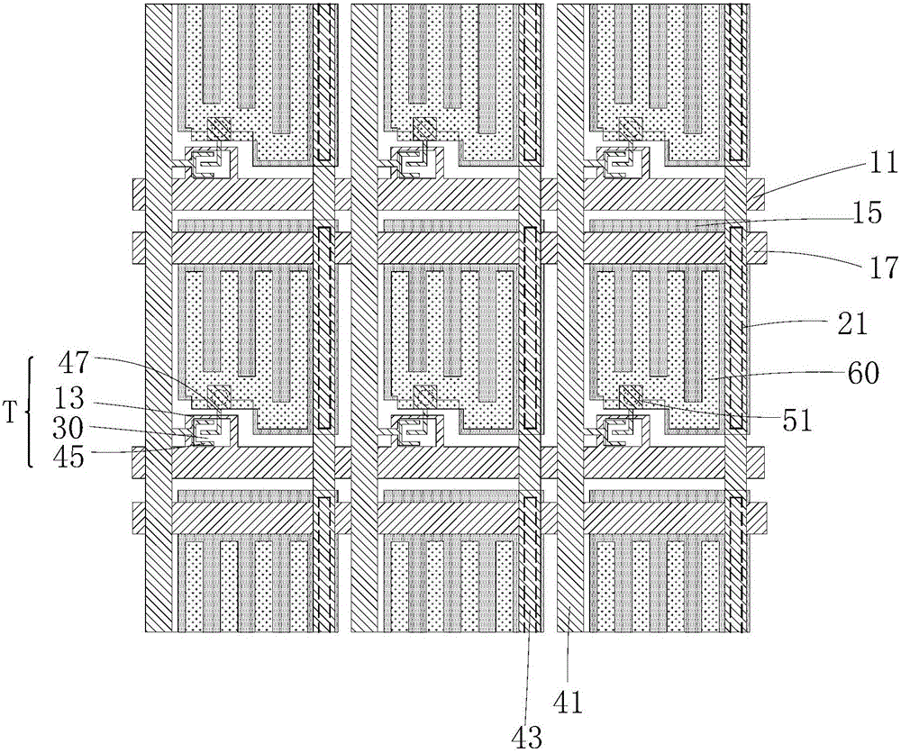
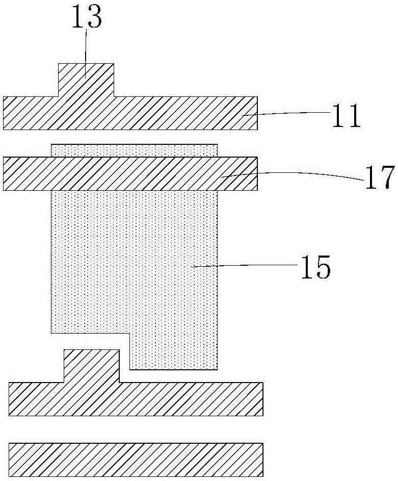
[0053] see figure 1 , the present invention firstly provides a TFT array substrate structure, comprising:

[0054] A plurality of grid scanning lines 11 arranged at intervals along the horizontal direction;

[0055] A plurality of data lines 41 arranged at intervals in the vertical direction, the plurality of gate scanning lines 11 arranged at intervals in the horizontal direction and a plurality of data lines 41 arranged at intervals in the vertical direction are insulated and interlaced with each other, dividing a plurality of sub-pixels area;

[0056] A plurality of common electrodes 15 arranged in a matrix, each common electrode 15 is correspondingly located in a sub-pixel area, and the common electrodes 15 in this embodiment are in the ...


PUM


Abstract

The invention provides a TFT array substrate structure and a manufacturing method thereof. The TFT array substrate structure is provided with a plurality of transverse common electrode wires (17) and a plurality of longitudinal common electrode wires (43), the transverse common electrode wires (17) correspond to each row of common electrodes (15) and are used for being connected with the common electrodes (15) in rows, the longitudinal common electrode wires (43) correspond to each line of common electrodes (15) and are used for being connected with the common electrodes (15) in lines, and the transverse common electrode wires (17) and the longitudinal common electrode wires (43) are interwoven to be in a net shape. Common voltages can be distributed more evenly in a liquid crystal display panel, and the image display quality of the liquid crystal display panel can be improved.

Description

technical field [0001] The invention relates to the technical field of liquid crystal display, in particular to a structure of a TFT array substrate and a manufacturing method thereof. Background technique [0002] A liquid crystal display (Liquid Crystal Display, LCD) has many advantages such as a thin body, power saving, and no radiation, and has been widely used. Such as: LCD TV, mobile phone, personal digital assistant (PDA), digital camera, computer screen or notebook computer screen, etc., occupy a dominant position in the field of flat panel display. [0003] Most of the liquid crystal displays currently on the market are backlight liquid crystal displays, which include a liquid crystal display panel and a backlight module. The working principle of the liquid crystal display panel is to pour liquid crystal molecules between the thin film transistor array substrate (ThinFilmTransistorArraySubstrate, TFTArraySubstrate) and the color filter substrate (ColorFilter, CF), ...

Claims


Application Information

Patent Timeline
Patent Type & Authority Applications(China)
IPC IPC(8): G02F1/1362G02F1/1343
CPCG02F1/134309G02F1/136286G02F2201/121G02F1/136295
Inventor 徐向阳
Owner TCL CHINA STAR OPTOELECTRONICS TECH CO LTD
Why Eureka
Try Eureka