Pixel circuit and driving method thereof, array substrate and display device

A technology of a pixel circuit and a driving method, which is applied in the display field, can solve the problems of OLED brightness uniformity, AMOLED luminous unevenness, etc., and achieve the effects of improving uniformity and display quality, improving picture uniformity, and compensating for non-uniformity.

Inactive Publication Date: 2015-11-25
BOE TECH GRP CO LTD +1
View PDF7 Cites 22 Cited by
  • Summary
  • Abstract
  • Description
  • Claims
  • Application Information

AI Technical Summary

Problems solved by technology

[0006] The present invention aims at the change of the threshold voltage of the existing driving transistor affecting the brightness uniformity of the OLED and the driving of the driving transistor T caused by the leakage of the switching transistor. D The problem of uneven luminescence of AMOLED caused by the change of the driving voltage of the gate provides a pixel circuit and its driving method, an array substrate, and a display device

Method used


Image

  • Pixel circuit and driving method thereof, array substrate and display device
  • Pixel circuit and driving method thereof, array substrate and display device
  • Pixel circuit and driving method thereof, array substrate and display device

Examples


Embodiment 1

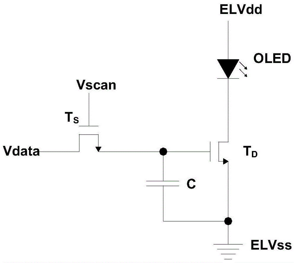
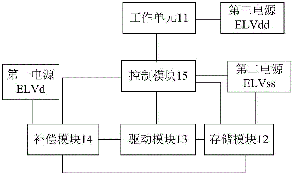
[0052] Such as image 3 As shown, this embodiment provides a pixel circuit, including: a working unit 11, a storage module 12, a driving module 13, a compensation module 14 and a control module 15, and the driving module 13 is connected to the control module 15, the compensation module 14 and the storage module 12 , the control module 15 is connected with the working unit 11, the compensation module 14, the drive module 13, the storage module 12 and the signal input terminal ELVss, the compensation module 14 is connected with the control module 15, the drive module 13, the storage module 12 and the first power supply ELVd, and stores The module 12 is connected to the compensation module 14, the driving module 13, the control module 15 and the signal input terminal ELVss, and the working unit 11 is connected to the control module 15 and the third power supply ELVdd;

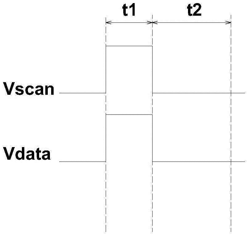
[0053] In the initialization phase, the compensation module 14 and the driving module 13 are initialized under ...

Embodiment 2

[0058] Such as Figure 4 As shown, this embodiment provides a pixel circuit, including: a working unit 11, a storage module 12, a driving module 13, a compensation module 14 and a control module 15, and the driving module 13 is connected to the control module 15, the compensation module 14 and the storage module 12 , the control module 15 is connected with the working unit 11, the compensation module 14, the drive module 13, the storage module 12 and the signal input terminal ELVss, the compensation module 14 is connected with the control module 15, the drive module 13, the storage module 12 and the first power supply ELVd, and stores The module 12 is connected to the compensation module 14, the driving module 13, the control module 15 and the signal input terminal ELVss, and the working unit 11 is connected to the control module 15 and the third power supply ELVdd;

[0059] In the initialization phase, the compensation module 14 and the driving module 13 are initialized under...

Embodiment 3

[0081] Such as image 3 , Figure 4 As shown, this embodiment provides a driving method for a pixel circuit. The pixel circuit includes: a working unit 11, a storage module 12, a driving module 13, a compensation module 14, and a control module 15. The driving module 13, the control module 15, and the compensation module 14 It is connected with the storage module 12, the control module 15 is connected with the working unit 11, the compensation module 14, the drive module 13, the storage module 12 and the signal input terminal ELVss, the compensation module 14 is connected with the control module 15, the drive module 13, the storage module 12 and the first The power supply ELVd is connected, the storage module 12 is connected with the compensation module 14, the driving module 13, the control module 15 and the signal input terminal ELVss, and the working unit 11 is connected with the control module 15 and the third power supply ELVdd;

[0082] The drive method includes:

[00...


PUM


Abstract

The invention provides a pixel circuit and a driving method thereof, an array substrate and a display device, belongs to the technical field of display, and can solve the problems that the threshold voltage change of an existing driving transistor influences the brightness uniformity of an OLED (Organic Light Emitting Diode) and an AMOLED (Active Matrix / Organic Light Emitting Diode) does not emit light uniformly due to the driving voltage change of the gate of the driving transistor caused by electric leakage of a switching transistor. The pixel circuit comprises a working unit, a storage module, a driving module, a compensation module and a control module; at the initialization phase, the compensation module and the driving module are initialized under the control of a first power supply; at the data write-in and compensation phase, a data signal input end charges the storage module through the compensation module; and at the display phase, the control module is enabled, and the storage module discharges electricity to the working unit through the driving module, so that the working unit emits light, and the influence of the threshold voltage drift of the driving module on the performance of the working unit is reduced.

Description

technical field [0001] The invention belongs to the field of display technology, and in particular relates to a pixel circuit, a driving method thereof, an array substrate, and a display device. Background technique [0002] With the advancement of display technology, more and more active matrix organic light emitting diode (Active Matrix Organic Light Emitting Diode, AMOLED) display panels have entered the market. Compared with traditional transistor liquid crystal display panels (ThinFilmTransistorLiquidCrystalDisplay, TFTLCD), AMOLED display panels have faster response Speed, higher contrast and wider viewing angle, therefore, AMOLED is getting more and more attention from panel manufacturers. [0003] figure 1 The circuit diagram for the existing AMOLED pixel structure, from figure 1 It can be seen from the figure that the AMOLED circuit diagram includes two thin film transistors T D and T S , storage capacitor C and an OLED, where T S The gate is connected to the s...

Claims


Application Information

Patent Timeline
Patent Type & Authority Applications(China)
IPC IPC(8): G09G3/32
CPCG09G2300/0842G09G2300/0861G09G2310/08G09G3/3233G09G2300/0819G09G2310/0251G09G2320/0233G09G2320/045G09G3/3258G09G3/3266G09G3/3275
Inventor 胡祖权
Owner BOE TECH GRP CO LTD
Why Eureka
Try Eureka