
Power Semiconductor Device of Stripe Cell Geometry

一种功率半导体、线型的技术,应用在半导体器件、电气元件、晶体管等方向,能够解决影响保护环结构耐受电压、周围电场分布不均匀、环状掺杂区缺口等问题

Active Publication Date: 2015-11-25
UPI SEMICON CORP
View PDF5 Cites 0 Cited by
  • Summary
  • Abstract
  • Description
  • Claims
  • Application Information

AI Technical Summary

Problems solved by technology

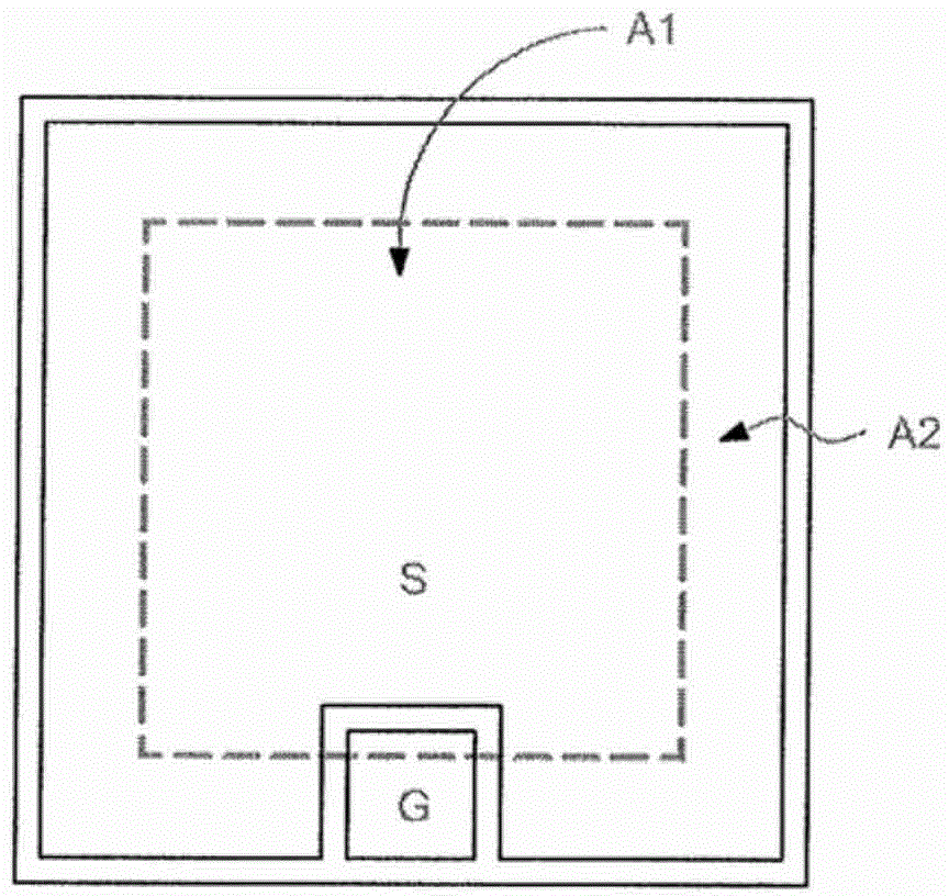
[0007] The main purpose of the present invention is to provide a power semiconductor element with a linear structure to solve the problem caused by the uneven electric field distribution around the active area of ​​the power semiconductor element with a traditional linear structure
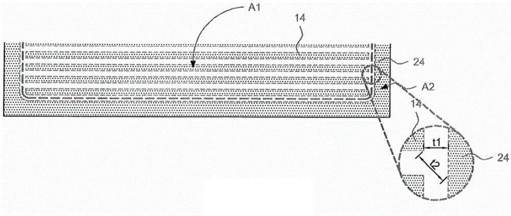
[0008] Another object of the present invention is to provide a power semiconductor element with a linear structure to solve the problem of gaps in the annular doped region caused by the existence of polysilicon gate busbars in the terminal area of ​​traditional power semiconductor elements, thereby affecting protection. The problem of the withstand voltage of the ring structure

Method used


Image

  • Power Semiconductor Device of Stripe Cell Geometry
  • Power Semiconductor Device of Stripe Cell Geometry
  • Power Semiconductor Device of Stripe Cell Geometry

Examples


Embodiment Construction

[0071] Reference will now be made in detail to the exemplary embodiments of the present invention, examples of which are illustrated in the accompanying drawings. In addition, elements / members with the same or similar numbers used in the drawings and the detailed description are used to represent the same or similar parts.

[0072] In the following embodiments, when an element is referred to as being “connected” or “coupled” to another element, it may be directly connected or coupled to the other element, or there may be intervening elements. The term "circuitry" may refer to at least one element or a plurality of elements, or elements that are actively and / or passively coupled together to provide a suitable function. The term "signal" may refer to at least one current, voltage, load, temperature, data or other signal.

[0073] Figure 2A to Figure 2E It is the first embodiment of the power semiconductor element of the present invention. The power semiconductor element is c...


PUM


Abstract

A power semiconductor device of stripe cell geometry including a substrate, a plurality of striped power semiconductor units, and a guard ring structure is provided. The substrate has an active area and a termination area surrounding the active area defined thereon. The striped semiconductor unit includes a striped gate conductive structure. The striped semiconductor units are located in the active area. The guard ring structure is located in the termination area and includes at least a ring-shaped conductive structure surrounding the striped power semiconductor units. The ring-shaped conductive structure and the striped gate conductive structures are formed on the same conductive layer, and at least one of the striped gate conductive structures is separated from the nearby ring-shaped conductive structure and electrically connected to the nearby ring-shaped conductive structure through the gate metal pad.

Description

technical field [0001] The present invention relates to a power semiconductor element, in particular to a power semiconductor element with a linear structure. Background technique [0002] Power semiconductor components have the advantages of low switching loss and simple driving circuit, and with the rapid development of semiconductor process technology, they have become an important product for power control. Power semiconductor devices can be classified into trench gate and planar gate according to the position of the channel. The channel of the trench gate power semiconductor structure is along the direction perpendicular to the wafer surface, while the channel of the planar gate power semiconductor structure is along the direction of the wafer surface. Secondly, power semiconductor devices can also be divided into squared cell and striped cell according to the different design methods of their unit cells. These two cell designs each have their advantages and disadvant...

Claims


Application Information

Patent Timeline
Patent Type & Authority Applications(China)
IPC IPC(8): H01L29/06H01L29/423
CPCH01L29/0619H01L29/0696H01L29/404H01L29/4238H01L29/7811H01L29/7813H01L27/088H01L29/0692
Inventor 涂高维蔡依芸张渊舜
Owner UPI SEMICON CORP
Learn More