Color film substrate and manufacturing method thereof
The technology of a color filter substrate and a manufacturing method, which is applied to the field of liquid crystal display screens, can solve the problems of increasing the number of photomask channels, complicated manufacturing processes, and difficulty in production, and achieves the effects of reducing the number of photomask channels and improving the shading effect.
- Summary
- Abstract
- Description
- Claims
- Application Information
AI Technical Summary
Problems solved by technology
Method used
Image
Examples
Embodiment 1
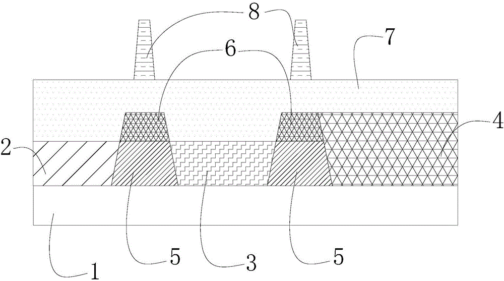
[0027] Such as figure 1 As shown, it is a schematic cross-sectional structure diagram of a color filter substrate of the present invention, from figure 1 It can be seen that a color filter substrate in this embodiment includes a glass substrate 1 , a color filter layer formed on the glass substrate 1 , and a flat layer 7 formed on the color filter layer.
[0028] Wherein, the glass substrate 1 is provided with a light-shielding area and a light-transmitting area, and the color filter layer includes a first color-resist layer 2, a second color-resist layer 3, and a third color-resist layer formed on the glass substrate 1. Layer 4, a first light-shielding layer 5 and a second light-shielding layer 6, the first light-shielding layer 5 covers the light-shielding area, the second light-shielding layer 6 covers the first light-shielding layer 5, the The first light-shielding layer 5 and the second light-shielding layer 6 form an overlapping light-shielding layer, the overlapping li...
Embodiment 2
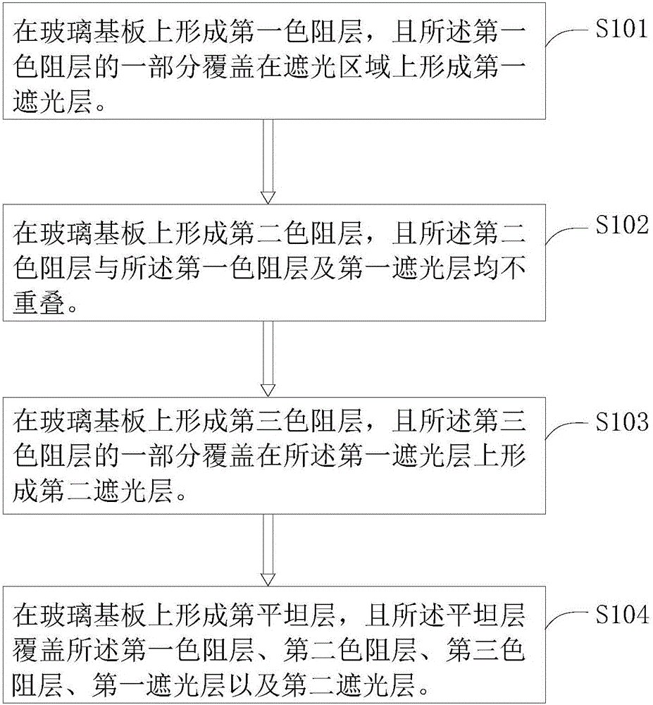
[0037] A method for manufacturing a color filter substrate in this embodiment includes:
[0038] The first color-resist layer 2, the second color-resist layer 3 and the third color-resist layer 4 are sequentially formed on the glass substrate, and the first color-resist layer 2, the second color-resist layer 3 and the third The color resist layer 4 covers the light-transmitting area of the glass substrate 1 .
[0039] Wherein, when forming the first color-resist layer 2 and forming the second color-resist layer 3, one of the color-resist layers in the first color-resist layer 2 or the second color-resist layer 3 A part of the first light-shielding layer 5 is formed on the light-shielding area of the glass substrate 1. When the third color-resisting layer 4 is formed, a part of the third color-resisting layer 4 covers the first light-shielding layer 5 The second light-shielding layer 6 is formed on it, and the light-shielding area is the area between the first color-resist...
PUM
 Abstract
Description
Claims
Application Information

