A charge pump circuit
A charge pump and voltage detection circuit technology, applied in the field of circuits, can solve the problems of waste of power consumption and unstable output voltage, and achieve the effect of reducing waste of power consumption and stable output voltage
- Summary
- Abstract
- Description
- Claims
- Application Information
AI Technical Summary
Problems solved by technology
Method used
Image

Examples
Embodiment 1
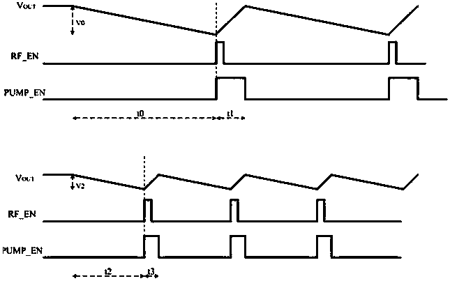
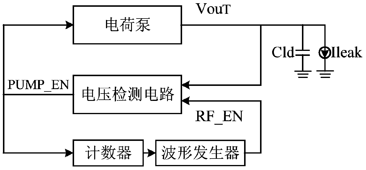
[0015] figure 1 It is a block diagram of a charge pump circuit provided by Embodiment 1 of the present invention, and this embodiment is applicable to low power consumption integrated circuits. A block diagram of a charge pump circuit provided in this embodiment, such as figure 1 As shown, it includes a voltage detection module, which is used to detect the output voltage of the charge pump under the control of the pulse signal, and outputs an enable signal to the charge pump, and starts the charge pump to start working; a counter is used to check the enable signal The enable period is timed, and when the enable period is lower than or higher than the set value, the frequency of the pulse signal generated by the waveform generator is adjusted; the waveform generator is used to generate the pulse signal to the voltage detection circuit under the control of the counter Refresh the detection frequency of the voltage detection circuit; the charge pump is used to output the target ...
Embodiment 2
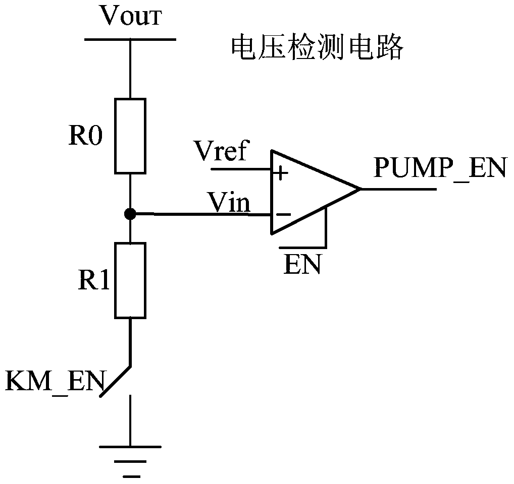
[0023] On the basis of the above embodiments, as a preferred embodiment, image 3 The specific circuit diagram of the voltage detection circuit is given, as image 3 As shown: the voltage detection circuit is composed of a first resistor R0, a second resistor R1, a comparator D1, and an enabling switch KM_EN; wherein the first resistor R0 and the second resistor R2 are connected in series and one end is connected to the enabling switch The energy switch KM_EN is connected, and the other end is connected to the output terminal Vout of the charge pump; the non-inverting input terminal of the comparator D1 inputs the reference voltage Vref, and the inverting input terminal is connected to Vin between the first resistor and the second resistor. , the output end outputs the enable signal PUMP_EN.
[0024] Wherein, the reference voltage Vref is a set value, the enable switch KM_EN is a normally open switch, and only when the voltage detection circuit starts to detect the output vol...
PUM
 Abstract
Description
Claims
Application Information
 - R&D
- Intellectual Property
- Life Sciences
- Materials
- Tech Scout
- Unparalleled Data Quality
- Higher Quality Content
- 60% Fewer Hallucinations
Browse by: Latest US Patents, China's latest patents, Technical Efficacy Thesaurus, Application Domain, Technology Topic, Popular Technical Reports.
© 2025 PatSnap. All rights reserved.Legal|Privacy policy|Modern Slavery Act Transparency Statement|Sitemap|About US| Contact US: help@patsnap.com