

Array substrate and production method thereof, as well as display device
A technology of an array substrate and a manufacturing method, which is applied in nonlinear optics, instruments, optics, etc., can solve the problem that the shading area cannot be effectively used, and achieve the effect of effective utilization
- Summary
- Abstract
- Description
- Claims
- Application Information
AI Technical Summary
Problems solved by technology
Method used
Image

Examples
Embodiment 1
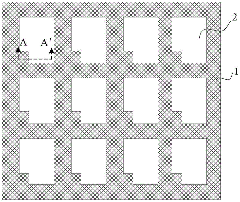
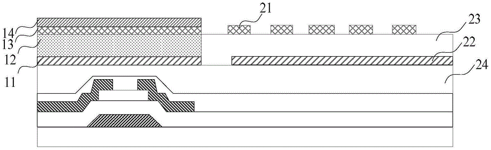
[0026] Embodiments of the present invention provide an array substrate, such as figure 1 and figure 2 As shown, the array substrate includes a plurality of light-transmitting regions 2, and a light-shielding region 1 surrounding each light-transmitting region 2. The light-shielding region 1 includes a first electrode 11, a photoelectric conversion film 12, and a second electrode 13 stacked in sequence. , the first electrode 11, the photoelectric conversion film 12 and the second electrode 13 constitute a photoelectric conversion unit, wherein the first electrode 11 is a transparent electrode.
[0027] It should be noted that the photoelectric conversion film 12 includes an N-type semiconductor film and a P-type semiconductor film, and the N-type semiconductor film and the P-type semiconductor film form a PN junction; in addition, the photoelectric conversion film 12 can also include an N-type semiconductor film and a P-type The I-type semiconductor film between the semicondu...
Embodiment 2
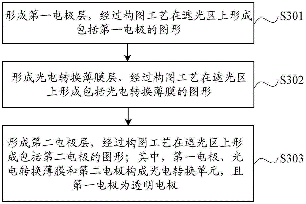
[0044] An embodiment of the present invention provides a method for fabricating an array substrate. The array substrate includes a plurality of light-transmitting regions and a light-shielding region surrounding each light-transmitting region, such as image 3 As shown, the method includes:
[0045] Step S301, forming a first electrode layer, and forming a pattern including the first electrode on the light-shielding region through a patterning process. Exemplarily, a first electrode layer is formed by methods such as plasma-enhanced chemical vapor deposition, sputtering or thermal evaporation, a photoresist is coated on the first electrode layer, and a mask plate having a pattern of the first electrode is used to cover The first electrode layer coated with photoresist is subjected to exposure, development, etching and other steps to form a pattern including the first electrode on the light-shielding area.
[0046] Step S302, forming a photoelectric conversion thin film layer,...
PUM
 Abstract
Description
Claims
Application Information