Unlock instant, AI-driven research and patent intelligence for your innovation.

Display substrate, manufacturing method thereof and display device

A technology for a display substrate and a manufacturing method, which is applied to optics, instruments, electrical components, etc., can solve the problems of thick thickness, poor flatness, influence, etc., so as to reduce the production cost, avoid the column spacer being too high, and simplify the manufacturing process. Effect

Inactive Publication Date: 2015-12-23
BOE TECH GRP CO LTD +1
View PDF6 Cites 14 Cited by
  • Summary
  • Abstract
  • Description
  • Claims
  • Application Information

AI Technical Summary

Problems solved by technology

[0005] From the above, it can be seen that in the prior art, two coating and exposure and development processes are required to form the black matrix structure 102 and the columnar spacers 105, because the exposure and development process is relatively cumbersome, so the cost increases accordingly
In addition, in order to solve this problem in the prior art, a layer of black matrix material is coated on the substrate, and then the black matrix structure 102 and the columnar spacers 105 are formed through a patterning process, such as figure 2 As shown; in this process, because the optical density value of the black matrix material is relatively small, the thickness of the formed black matrix structure 102 and columnar spacer 105 is relatively thick, and the flatness is poor, which will cause adverse effects on the subsequent box alignment process , resulting in poor display of the panel

Method used


Image

  • Display substrate, manufacturing method thereof and display device
  • Display substrate, manufacturing method thereof and display device
  • Display substrate, manufacturing method thereof and display device

Examples


Embodiment Construction

[0053] Embodiments of the present invention provide a display, a manufacturing method thereof, and a display device, which are used to simplify the manufacturing process and reduce production costs, while improving panel display quality.

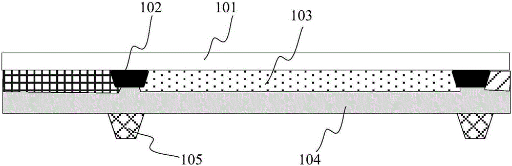
[0054] Embodiment 1 of the present invention provides a method for manufacturing a display substrate, see image 3 ; the method comprising:

[0055] Step 301, see Figure 3a , forming a non-transparent material layer 31 for making a black matrix on the base substrate 30;

[0056] Step 302, see Figure 3b , forming a transparent material layer 32 for making main and auxiliary columnar spacers on the substrate after completing the above steps;

[0057] Step 303, see Figure 3c , using a patterning process to form a pattern including the main column spacer 33 , the sub-column spacer 34 and the black matrix 35 .

[0058] In the manufacturing method of the display substrate provided in Embodiment 1 of the present invention, a non-transparent...


PUM


Abstract

The invention provides a display substrate, a manufacturing method thereof and a display device. The manufacturing technology is simplified, the production cost is reduced, and meanwhile the panel display quality is improved. The manufacturing method comprises the steps that a nontransparent material layer used for manufacturing a black matrix is formed on a substrate base, and then a transparent material layer used for manufacturing main and auxiliary columnar isolating pads is formed on the substrate base; a picture comprising the main and auxiliary columnar isolating pads and the black matrix is formed through the picture composition technology, and the segment difference between the main and auxiliary columnar isolating pads is 0.3-0.7 micrometers.

Description

technical field [0001] The invention relates to the field of display technology, in particular to a display substrate, a manufacturing method thereof, and a display device. Background technique [0002] Thin Film Transistor-Liquid Crystal Display (hereinafter referred to as: TFT-LCD) has become the mainstream of flat-panel displays due to its low power consumption, relatively low manufacturing cost and no radiation, and is widely used in various display components such as mobile On the monitors of electronic devices such as phones, personal digital assistants (Personal Digital Assistants, PDAs), computers, and televisions. Its working principle is mainly to use the electric field to control the arrangement state of the liquid crystal molecules, whether the light generated by the backlight can pass through the liquid crystal molecules to achieve the light and dark display effect on the display screen. [0003] The TFT-LCD panel is composed of a color filter substrate and an ...

Claims


Application Information

Patent Timeline
Patent Type & Authority Applications(China)
IPC IPC(8): G02F1/1339G02F1/1335
CPCG02F1/133512G02F1/13394G02F1/13396H01L27/1248H01L27/1259H01L27/1288G02F1/13398G02F1/136236G02F1/136222G02F1/1368H01L27/1222
Inventor 唐文浩陆相晚李宾袁慧芳朱涛尹海斌陈建董安鑫方群钟国强傅欣欣
Owner BOE TECH GRP CO LTD