Touch display device and touch substrate

A touch display device and substrate technology, applied in optics, instruments, electrical digital data processing, etc., can solve the problems affecting the visibility of touch display devices, large RC load of sensing electrodes, and affecting signal transmission, etc., to achieve Excellent impedance matching, reduced RC load, and high visibility

Inactive Publication Date: 2015-12-23
INNOLUX CORP
View PDF6 Cites 3 Cited by
  • Summary
  • Abstract
  • Description
  • Claims
  • Application Information

AI Technical Summary

Problems solved by technology

However, if the overall line width of the bridged metal layer is large, although the RC loading of the sensing electrode can be made smaller and will not affect signal transmission, however, since the metal layer is generally an opaque material, Therefore, the visibility of the touch display device will be affected; in addition, if the overall line width of the bridged metal layer is small, although the visibility of the touch display device will not be affected, the RC load of the sensing electrode will be too much. large enough to affect its signal transmission

Method used


Image

  • Touch display device and touch substrate
  • Touch display device and touch substrate
  • Touch display device and touch substrate

Examples


Embodiment Construction

[0027] The touch display device and the touch substrate according to preferred embodiments of the present invention will be described below with reference to related drawings, wherein the same elements will be described with the same reference symbols. The illustrations of all the implementation aspects of the present invention are only schematic representations, and do not represent real dimensions and proportions.

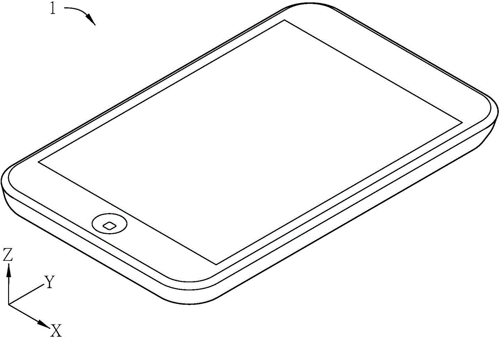
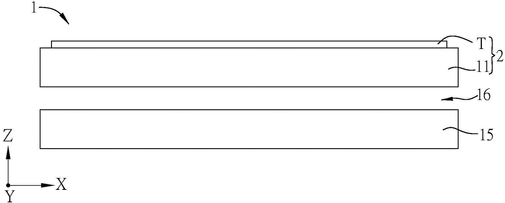
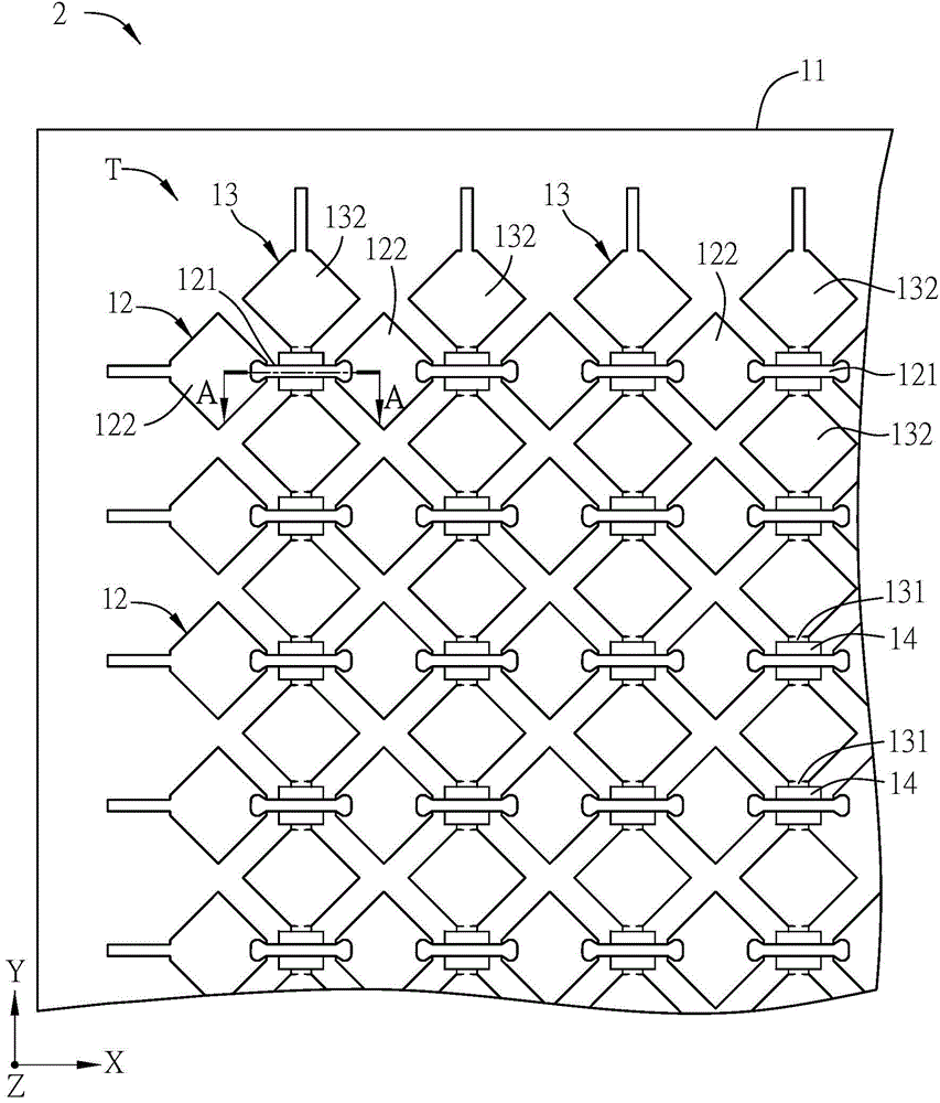
[0028] Please refer to Figure 1A to Figure 1E As shown, among them, Figure 1A It is a schematic diagram of a touch display device 1 according to a preferred embodiment of the present invention, Figure 1B is a schematic cross-sectional view of the touch display device 1, Figure 1C for Figure 1B A top view schematic diagram of a touch substrate 2, Figure 1D for Figure 1C In the touch substrate 2, the schematic cross-sectional view along the line A-A, and Figure 1E for Figure 1D top view diagram.

[0029] For ease of description, this embodiment show...


PUM


Abstract

First touch patterns of a touch display device are disposed on a first substrate, and have bridge units and first electrode portions. The first electrode portions are disposed spaced from each other. The bridge units are connected with adjacent two of the first electrode portions. A second substrate is disposed opposite to the first substrate. A liquid crystal layer is disposed between the first substrate and the second substrate. One of the bridge units has two first portions, a second portion and two third portions. The first portions are located on the first electrode portions, and directly contact with the first electrode portions. The third portions are located on two of the first portions, and the second portion is located between two of the third portions. The first portion has a first width, and the second portion has a second width smaller than the first width.

Description

technical field [0001] The invention relates to a touch display device and a touch substrate. Background technique [0002] With the advancement of technology, touch technology has been widely used in various electronic products. For the touch display device, because the user can perform various functions by touching the display screen of the touch display device, it can simplify the complexity of the user's operation, and is more and more popular among consumers. . [0003] The touch display device generally includes an Out-Cell touch device or an On-Cell touch device. In the aspect of the plug-in touch device, the touch sensing circuit is formed on a substrate, and then combined with the display panel to form a touch display panel. In the aspect of the embedded touch device, the touch sensing circuit is directly formed on the light-transmitting substrate such as the color filter substrate, and combined with the thin film transistor substrate to form a touch display pane...

Claims


Application Information

Patent Timeline
Patent Type & Authority Applications(China)
IPC IPC(8): G06F3/041
CPCG06F3/047G02F1/13338G06F2203/04111G06F3/0446G06F3/0445
Inventor 陈志昌许苇亭陈扬证张嘉雄
Owner INNOLUX CORP
Why Eureka
Try Eureka