Grounding Pattern Structure For High-frequency Connection Pad Of Circuit Board

A graphic structure, high-frequency welding technology, applied in circuits, printed circuits, printed circuits, etc., can solve the problem of no high-frequency signal transmission, and achieve the effect of reducing the probability of high-frequency differential mode signal transmission errors and the effect of reducing the probability

Active Publication Date: 2014-09-24
ADVANCED FLEXIBLE CIRCUITS
View PDF6 Cites 2 Cited by
  • Summary
  • Abstract
  • Description
  • Claims
  • Application Information

AI Technical Summary

Problems solved by technology

However, at the connection between the differential-mode signal line and the high-frequency pad area arranged on the circuit board and the adjacent area, due to the line width (very small line width) of the differential-mode signal line and the signal guide pin of the connector and zero Due to the limitation of component size specification (relative to the line width of the signal line, the size is relatively large), so far, there is no effective solution for the industry in this technical field to ensure the quality of high-frequency signal transmission
[0008] In addition, in the application where the circuit board is plugged into the slot of a connector base and a connector is arranged on the circuit board, the differential mode signal line and the high-frequency pad area are connected to the conductive terminals of the connector base. , The quality of high-frequency signal transmission between the signal guide pins of the connector, so far there is no feasible and effective method to ensure

Method used


Image

  • Grounding Pattern Structure For High-frequency Connection Pad Of Circuit Board
  • Grounding Pattern Structure For High-frequency Connection Pad Of Circuit Board
  • Grounding Pattern Structure For High-frequency Connection Pad Of Circuit Board

Examples


Embodiment Construction

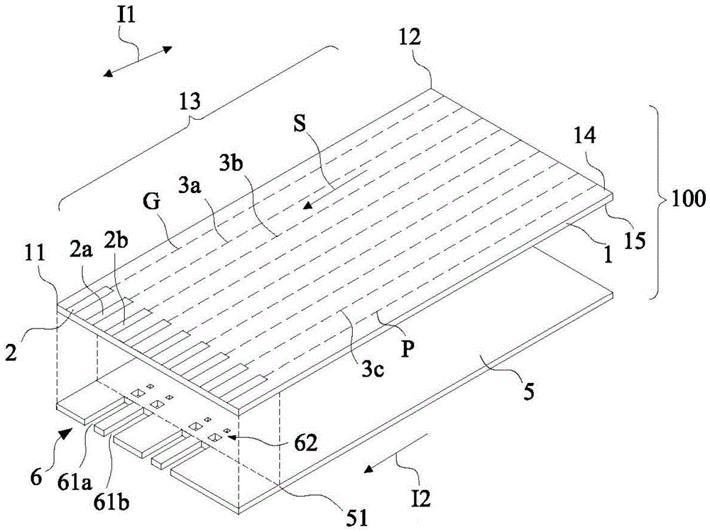
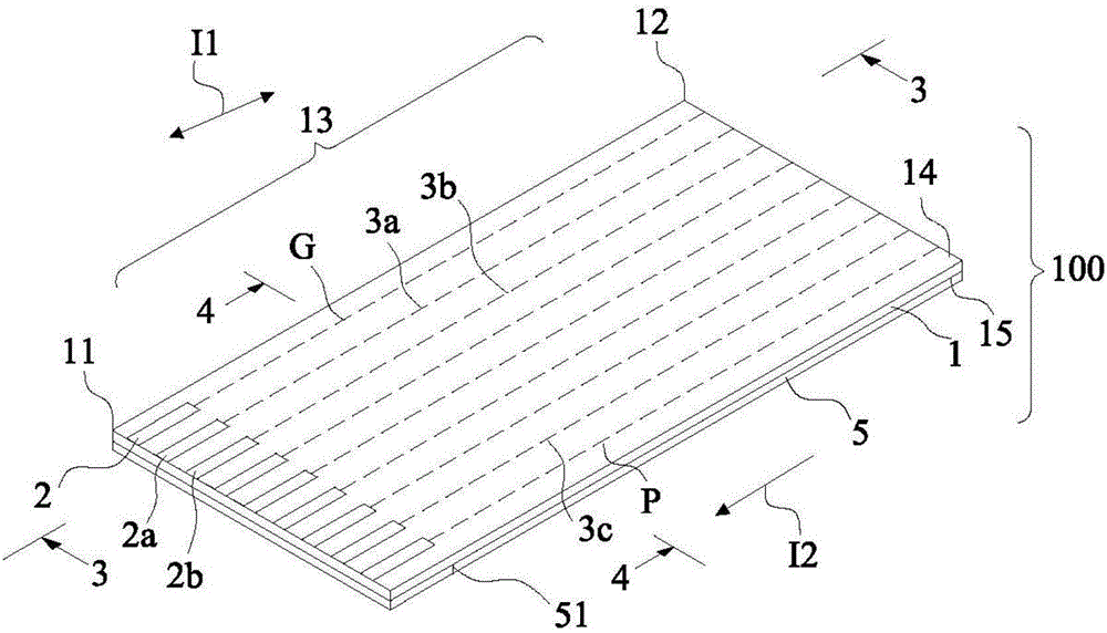
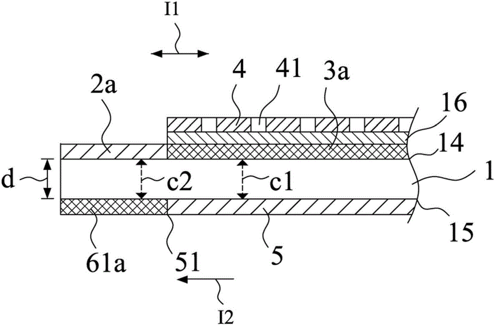
[0077] refer to Figure 1 ~ Figure 2 shown, where figure 1 shows an exploded perspective view of the first embodiment of the present invention, figure 2 A perspective view of a first embodiment of the invention is shown. The circuit board 100 of this embodiment includes a substrate 1, the substrate 1 has a first end 11, a second end 12, and an extending direction I1 between the first end 11 and the second end 12. An extension section 13 .

[0078] A plurality of pad regions 2 are arranged adjacent to each other and insulated on the device surface 14 of the substrate 1 , and adjacent to the first end 11 of the substrate 1 . Each pad area 2 includes at least one pair of high frequency pad areas 2a, 2b.

[0079] The extension section 13 is provided with at least one pair of differential-mode signal lines 3a, 3b for carrying at least one high-frequency differential-mode signal S. As shown in FIG. The differential mode signal lines 3a, 3b are respectively connected to the cor...


PUM


Abstract

Disclosed is a grounding pattern structure for high-frequency connection pads of a circuit board. A substrate of the circuit board includes a component surface on which at least a pair of high-frequency connection pads are arranged. At least a pair of differential mode signal lines are arranged on the substrate and connected to the high-frequency connection pads. The grounding surface of the substrate includes a grounding layer formed at a location corresponding to the differential mode signal lines. A first capacitive coupling is formed between the grounding layer and the differential mode signal lines. The grounding surface of the substrate includes a grounding pattern structure formed thereon to correspond to a location adjacent to the high-frequency connection pads. The grounding pattern structure is electrically connected to the grounding layer. A second capacitive coupling matching the first capacitive coupling is formed between the grounding pattern structure and the high-frequency connection pads. The component surface of the substrate can be provided with a connector mounted thereto with signal terminals of the connector soldered to the high-frequency connection pads. Accordingly, the probability of transmission errors of the high-frequency differential mode signal is reduced, and the transmission quality of the high-frequency signal is ensured.

Description

technical field [0001] The invention relates to a structural design for improving the transmission quality of high-frequency signals of a circuit board, in particular to a grounding pattern structure of a high-frequency welding pad area of ​​a circuit board. Background technique [0002] In all kinds of electronic devices used today, because the amount of data transmitted by signal lines is increasing, the number of signal transmission lines required is not only increasing, but the frequency of transmitting signals is also increasing. Differential Mode (Differential Mode) signal transmission technology to reduce electromagnetic interference (EMI), such as USB or LVDS (Low Voltage Differential Signaling) or EDP (Embedded Display Port) signals extensively use this transmission technology to reduce electromagnetic interference. [0003] In the technology of differential mode signal transmission, two differential mode signal lines are mainly used to form a signal pair to transmi...

Claims


Application Information

Patent Timeline
Patent Type & Authority Applications(China)
IPC IPC(8): H05K1/11H05K1/09
CPCH05K1/0219H01P3/02H05K1/0245H05K1/117H01P3/026H05K1/0224H05K1/0253H05K2201/058
Inventor 卓志恒林崑津苏国富
Owner ADVANCED FLEXIBLE CIRCUITS
Why Eureka
Try Eureka