Ball grid array millimeter wave broadband matching structure and design method in wafer level packaging

A technology of wafer-level packaging and ball grid array, which is applied in the direction of semiconductor/solid-state device parts, semiconductor devices, electrical components, etc., can solve problems such as signal line mismatch, achieve impedance matching, reduce return loss, Reduce the effect of the discontinuity

Active Publication Date: 2022-07-01
ANHUI UNIVERSITY
View PDF12 Cites 0 Cited by
  • Summary
  • Abstract
  • Description
  • Claims
  • Application Information

AI Technical Summary

Problems solved by technology

[0014] The invention realizes the broadband matching between the center signal BGA solder ball connection structure and the front-end circuit transmission line through the adjustment function of the multi-stage ladder impedance resonator, and solves the problem in the impedance compensation structure of the through-silicon via BGA interconnection in the three-dimensional wafer level packaging. The size of the bottom of the BGA solder ball is larger than the width of the signal line of the front-end circuit of the microwave dielectric substrate, which causes the impedance mismatch between the impedance compensation structure of the TSV BGA interconnection and the signal line of the front-end circuit

Method used


Image

  • Ball grid array millimeter wave broadband matching structure and design method in wafer level packaging
  • Ball grid array millimeter wave broadband matching structure and design method in wafer level packaging
  • Ball grid array millimeter wave broadband matching structure and design method in wafer level packaging

Examples


Embodiment 1

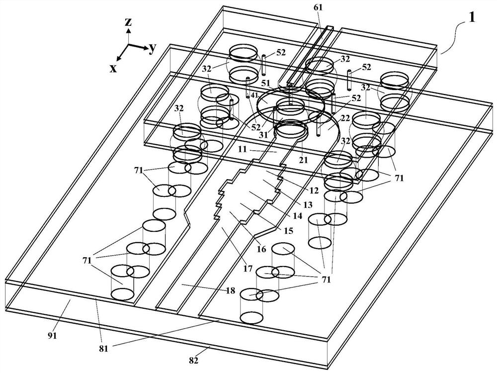
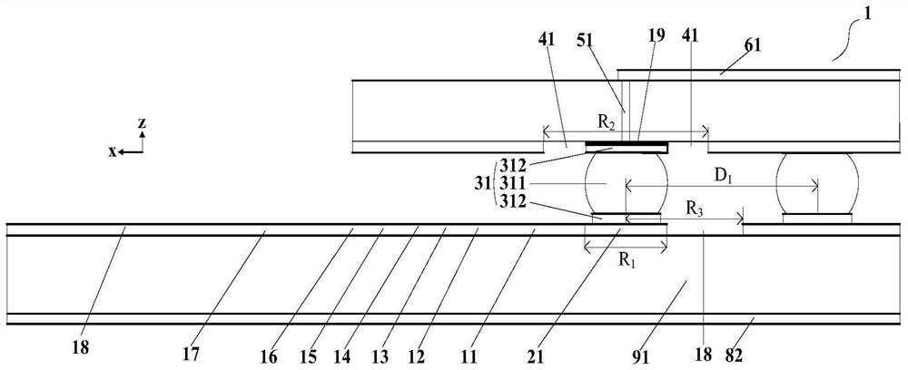
[0055] like figure 1 and figure 2 As shown, a ball grid array millimeter-wave broadband matching structure in wafer-level packaging includes a silicon-based chip 1, a microwave dielectric substrate 91, and metal ground plates 81 on both sides of the upper surface of the microwave dielectric substrate 91, located on the microwave dielectric substrate 91. The lower metal grounding plate 82 on the lower surface is used to connect the metal grounding plates 81 on both sides with the metal vias 71 of the lower metal grounding plate 82 , the circular metal plate 21 and the semicircular slot 22 on the upper surface of the microwave dielectric substrate 91 .

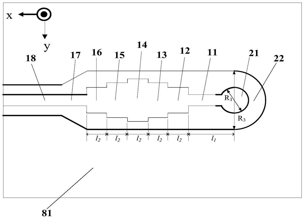
[0056] like figure 2 As shown, the upper surface of the microwave dielectric substrate 91 is sequentially connected along the positive direction of the x-axis to the first branch 11 signal line, the second branch 12 signal line, the third branch 13 signal line, the fourth branch 14 signal line, and the fifth branch. 15 signa...


PUM

PropertyMeasurementUnit
thicknessaaaaaaaaaa

Abstract

A ball grid array millimeter-wave broadband matching structure and design method in wafer-level packaging belong to the technical field of microwave and millimeter-wave packaging circuit systems. The upper surface of the microwave dielectric substrate is sequentially connected along the positive x-axis direction. Line, multi-stage stepped impedance resonator, front-end circuit transmission line; the millimeter wave signal output by the central signal BGA solder ball connection structure is transmitted to the multi-stage stepped impedance resonator through the first branch signal line to achieve broadband matching, and then the multi-stage stepped impedance The resonator is transmitted to the output of the front-end circuit transmission line, which realizes the broadband matching between the central signal BGA solder ball connection structure and the front-end circuit transmission line, and solves the problem of the BGA solder ball bottom in the through-silicon via BGA interconnect impedance compensation structure in the three-dimensional wafer-level packaging. The problem of impedance mismatch between the through-silicon via BGA interconnect impedance compensation structure and the signal line of the front-end circuit caused by the size being larger than the width of the signal line of the front-end circuit of the microwave dielectric substrate.

Description

technical field [0001] The invention belongs to the technical field of microwave and millimeter-wave packaging circuit systems, and in particular relates to a ball grid array millimeter-wave broadband matching structure and a design method in wafer-level packaging. Background technique [0002] With the rapid development of modern communication technology and radar technology, the circuit system is developing in the direction of high integration, high speed, miniaturization and low power consumption. The wavelength of the signal is of the same order of magnitude, which makes the signal present a wave effect on the transmission line, which adversely affects the signal transmission. Therefore, packaging has become a key factor restricting the development of high-frequency integrated circuits. The advanced three-dimensional wafer-level packaging interconnection provides a feasible technical solution to the bottleneck brought by the rapid development of miniaturized high-perfor...

Claims


Application Information

Patent Timeline
Patent Type & Authority Patents(China)
IPC IPC(8): H01L23/538H01L21/768
CPCH01L23/5386H01L23/5384H01L21/76898H01L21/76895
Inventor 朱浩然李坤吴博吴先良
Owner ANHUI UNIVERSITY
Why Eureka
Try Eureka