CMOS technology based broadband bidirectional RF amplifier

A bidirectional radio frequency and forward amplifier technology, applied in high frequency amplifiers, improved amplifiers to reduce noise impact, etc., can solve problems such as low linearity of single-pole double-throw switches, reduce LNA output power, limit circuit output power, etc., to achieve Effect of high isolation, elimination of noise figure and output power deterioration, and improvement of output power

Active Publication Date: 2018-02-23
安徽矽芯微电子科技有限公司
View PDF4 Cites 0 Cited by
  • Summary
  • Abstract
  • Description
  • Claims
  • Application Information

AI Technical Summary

Problems solved by technology

[0004] The first is that when working in the forward direction, the SPDT switching loss at the LNA input will increase the noise figure, and the output SPDT switching loss will reduce the LNA output power. From the perspective of the entire receiving chain, the two SPDT switches will make the LNA gain Reduce 2-3dB
[0005] The second is that when working in reverse, the PA output single-pole double-throw switch loss will reduce the PA output power. From the perspective of the entire transmission chain, two single-pole double-throw switches will reduce the PA gain by 2-3dB
[0006] Third, in the CMOS process, the linearity of the single-pole double-throw switch is not high. When the output power of the PA is large, the switch limits the output power of the circuit.
[0007] The fourth is that since the input and output have single-pole double-throw switch circuits, the layout area of ​​the chip is relatively large, which increases the cost of the chip

Method used


Image

  • CMOS technology based broadband bidirectional RF amplifier
  • CMOS technology based broadband bidirectional RF amplifier
  • CMOS technology based broadband bidirectional RF amplifier

Examples


Embodiment Construction

[0027] The present invention will be further described below in conjunction with accompanying drawing:

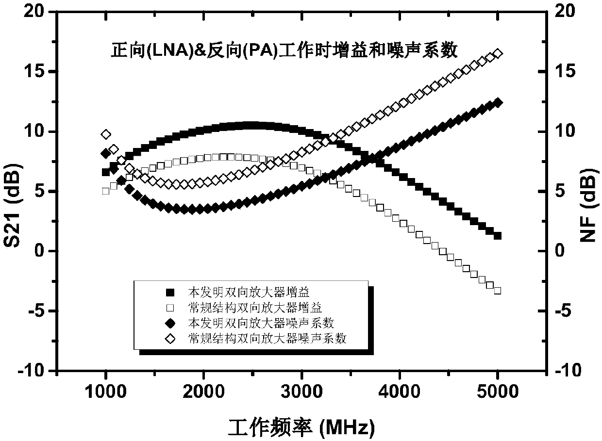
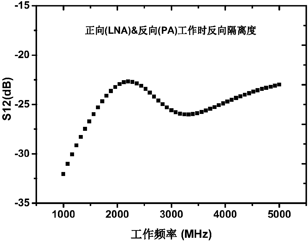
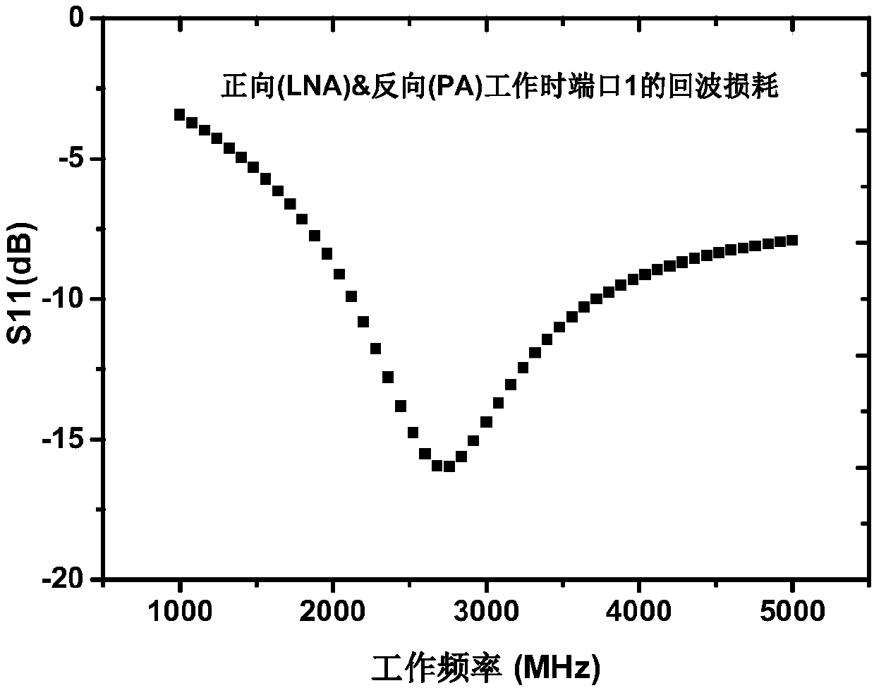
[0028] like figure 2 , image 3 , Figure 4 and Figure 5 As shown, the broadband bidirectional radio frequency amplifier based on CMOS technology described in the first embodiment includes a forward amplifier broadband LNA and a reverse amplifier broadband PA. Both the LNA and the PA adopt a common-source configuration circuit topology with RC negative feedback, and the LNA The RF input end of the LNA is connected with the RF output end of the PA, and the RF output end of the LNA is connected with the RF input end of the PA.

[0029] The forward amplifier broadband LNA includes a MOS tube M1 as a radio frequency amplifier tube, L B_R is the gate inductance, L S_R is the source negative feedback inductance, R 2_R and C 2_R It constitutes RC negative feedback to expand the bandwidth of the circuit, and also includes MOS tube M2 and MOS tube M3 to form switches respec...


PUM


Abstract

The invention discloses a CMOS technology based broadband bidirectional RF amplifier which can overcomes disadvantages of a traditional single-pole double-throw switch structure based bidirectional RFamplifier. The CMOS technology based broadband bidirectional RF amplifier comprises a forward amplifier broadband and a reverse amplifier broadband; both the forward amplifier broadband and the reverse amplifier broadband adopt a common-source configuration circuit topology which carries RC negative feedback; the RF input end of the forward amplifier broadband and the RF output end of the reverseamplifier broadband are connected together; and the RF output end of the forward amplifier broadband and the RF input end of the reverse amplifier broadband are connected together. The broadband bidirectional RF amplifier is realized based on the CMOS technology, is simple in circuit structure, can realize forward and reverse amplification and has relatively high isolation. The circuit structurecan be switched without a RF single-pole double-throw switch; the problems of noise coefficient and output power deterioration caused by switching consumption are removed; and broadband matching of two ports can be realized in a forward working mode and a reverse working mode.

Description

technical field [0001] The invention relates to a broadband bidirectional radio frequency amplifier circuit, in particular to a broadband bidirectional radio frequency amplifier based on CMOS technology. Background technique [0002] The RF amplifier circuit is one of the most common circuit units in the wireless transceiver system, and its function is to amplify the RF signal. For example, RF low-noise amplifiers are used to improve the detection ability of wireless transceivers for weak signals, and RF power amplifiers are used to increase the radiation distance of wireless transmitter signals. Most wireless systems need to implement receiving and transmitting functions at the same time, such as uplink and downlink on communication links, receiving links and transmitting links in electronic equipment such as radar. In order to improve system integration, simplify architecture, and reduce costs, bidirectional RF amplifiers are often required in these systems to amplify upl...

Claims


Application Information

Patent Timeline
Patent Type & Authority Applications(China)
IPC IPC(8): H03F1/26H03F3/19
CPCH03F1/26H03F3/19
Inventor 胡善文饶疆
Owner 安徽矽芯微电子科技有限公司
Why Eureka
Try Eureka