Multi-channel integrated circuit

a multi-channel integrated circuit and integrated circuit technology, applied in the field of multi-channel integrated circuits, can solve the problems of inability to read out conventional discrete or hybrid electronics, inability to achieve high inability to achieve good quantum efficiency for higher-energy x-rays and gamma rays, etc., to achieve fast trigger output, low noise, and the effect of handling large rates

Inactive Publication Date: 2007-03-15
NOVA R&D
View PDF15 Cites 24 Cited by
  • Summary
  • Abstract
  • Description
  • Claims
  • Application Information

AI Technical Summary

Benefits of technology

[0016] The design of the ASIC is guided by two principal goals. The first goal was to make the chip applicable to as wide a variety of applications as possible; this called for a flexible yet easy to use design. It has the ability to combine, on the same chip, signals that differ in terms of their polarity, rise time, threshold requirements, etc. This option, which is not available on the present RENA chip, enables users to optimize their system layout for the shortest possible signal connections, without regard to signal type. This contributed to achieving the second goal, which is equal in importance to the first, namely performance, for example, to obtain the best resolution possible for the combined detector-readout system. To reach this goal, we have designed the RENA-2 ASIC to achieve the lowest possible noise consistent with the characteristics of the detectors with which the ASIC is intended to be used.
[0018] The features include low-noise performance, self-trigger capability, several different peaking times, different readout modes, and the daisy-chain option. New innovative features, such as user-selectable dynamic ranges and the ability to provide channel-by-channel timing information, were added. These new features, as well as the significant performance improvements required a completely new design for the new developed ASIC. The design goal for the noise performance, in particular, represents a significant improvement over the present RENA chip and substantial innovation was required in order to reach this goal. Innovation was even more urgently needed to achieve improved noise performance while reducing the chip's power consumption.
[0020] Table 1 shows the main specifications for RENA-2 ASICs. These features include the chip's low-noise performance, its self-trigger capability, and the versatility it offers by providing several different peaking times, different readout modes, and the daisy-chain option. New, innovative features include low noise, self resetting charge sensitive input amplifier, selectable multi-range shaper, user-selectable dynamic ranges, fast trigger output for coincident event detection and the ability to provide channel-by-channel time difference information. The comparator thresholds will be individually adjustable through an 8 bit DAC on each channel. This will allow accurate and uniform threshold setting throughout the detector. Two very important new features for space deployment are the adjustable power consumption by limiting the current flow to the input transistor and the radiation hardness inherent to the 0.5 micron CMOS process. The peaking times were made adjustable from about 0.4 to 40 microseconds, which makes the chip suitable for a wide range of detectors, from CdZnTe to HgI2 as listed above. The new chip incorporates a pole zero cancellation circuit to handle large rates without significant pileup. The functionality of the new RENA ASIC is dramatically improved by eliminating unnecessary connections and interface. Another important new feature is the inclusion of 4 extra channels to allow the connection of the cathode side into the same ASIC. The input amplifier is made tolerant to leakage current so that the ASIC can be used DC coupled which eliminates the need to use capacitive coupling.

Problems solved by technology

Although an excellent detector, silicon, with an atomic number (Z) of 14, does not have good quantum efficiency for higher energy x-rays and gamma rays.
Although strongly promising high-Z position sensitive solid state detectors were developed, an essential component to make them viable instruments for detecting and imaging x-rays, gamma rays and particles has been missing.
Such detectors have many channels with small pitch, and reading them out with conventional discrete or hybrid electronics is not a viable option.
However, these chips lack two major functions, which are not needed for those experiments but render the chips mostly unsuitable for use in nuclear physics, astrophysics, and medical and industrial imaging:
In addition, the event trigger is typically based on the overall event topology rather than the signal levels in individual channels, which precludes its implementation on the readout chip.
Therefore, the application of position sensitive solid state detectors to nuclear and astrophysics and to medical and industrial imaging was largely delayed as a suitable ASIC readout chip was not available.
Also the RENA chip could only partially answer the requirements of many applications listed above.

Method used


Image

  • Multi-channel integrated circuit
  • Multi-channel integrated circuit
  • Multi-channel integrated circuit

Examples


Embodiment Construction

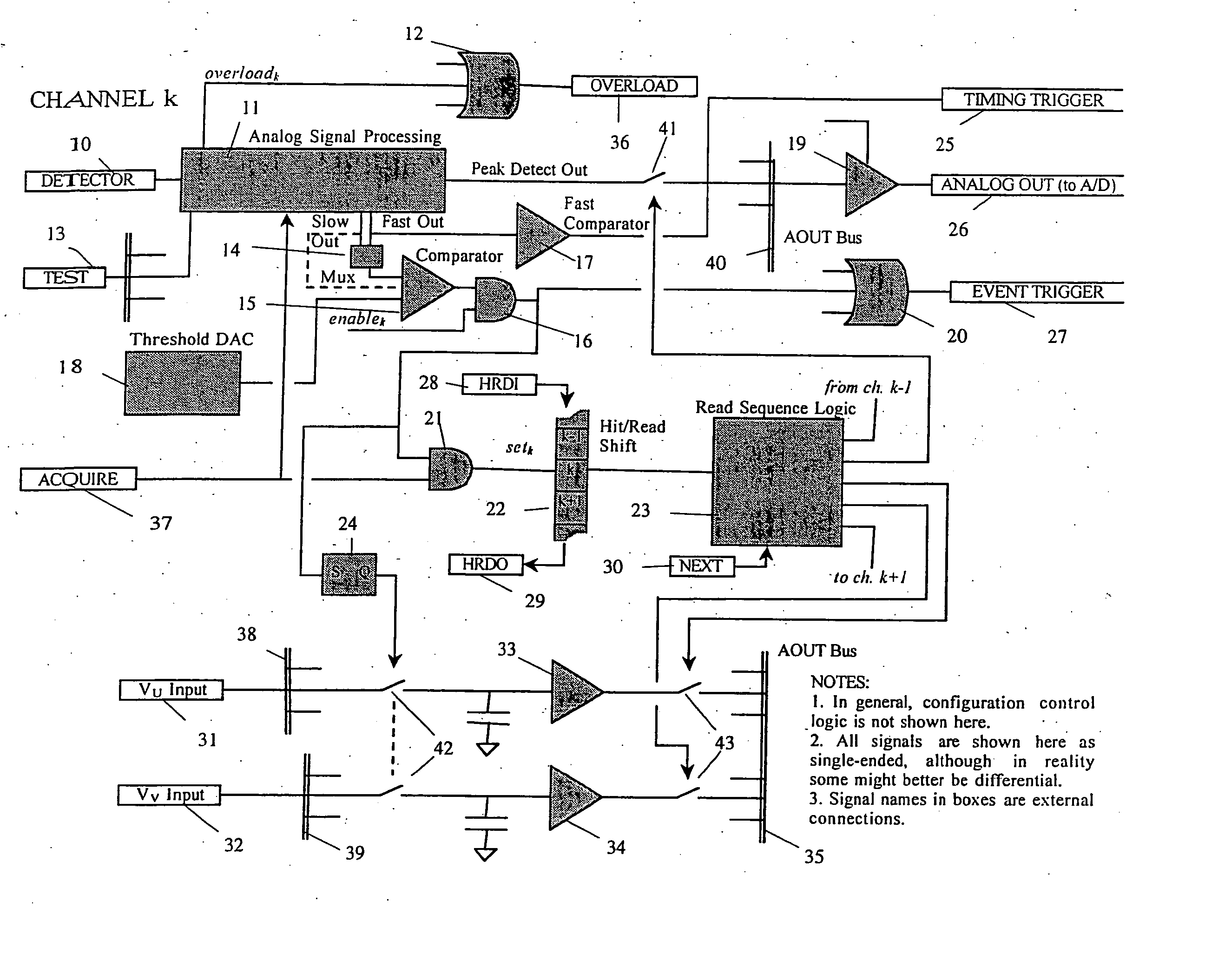
[0034] Referring to the ASIC described in FIG. 1 a detector 10 is connected to the input of the ASIC and the input goes to an analog signal processing unit 11. The FIG. 1 shows only one of the analog channels of the ASIC, the k channel. Analog processing unit is described below. Peak detector output of the analog signal processing unit 11 goes to analog output buffer amplifier 19 through a switch 41 controlled by read sequence logic 23. The peak detect output is also attached onto a bus 40 before it enters analog output buffer 19. Analog output is made available to the outside world as an output 26 of the ASIC. A test input 13 is used to test the analog signal processing unit. An overload sensing element 12 is connected to the analog signal processing unit 11. Output of the overload sensor 36 is provided to outside world as an output of the ASIC.

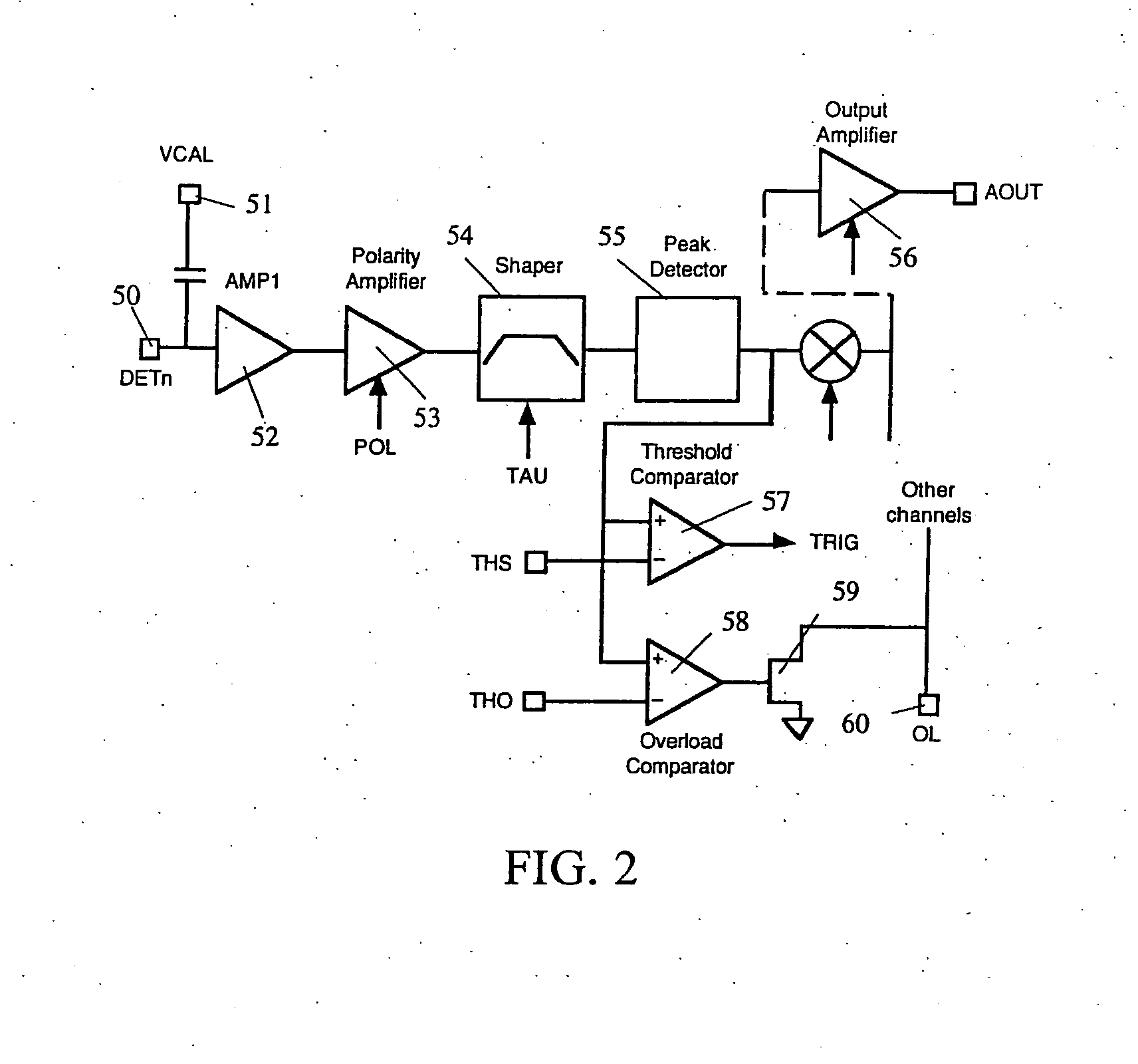
[0035] Analog signal processing unit 11 outputs a slow and fast shaper signal during processing of the signal from the detector 10 which g...


PUM


Abstract

A multi-channel integrated circuit is provided in which each channel has an analog section and a digital section. Each channel of the readout chip employs low noise charge sensitive amplifier at its input followed by other circuitry such as shaper, pole-zero, peak hold, different comparators, buffers and digital control and readout. Each channel produces a self-trigger and a fast timing output. Channel-to-channel time differences are also recorded. Integrated circuit also provides a large dynamic range to facilitate large range of applications. The trigger threshold can be adjusted to provide energy discrimination. The chip has different, externally selectable, operational modes including a sparse readout mode in which only the channels which have received signals greater than a preselected threshold value are read out. The sparse readout mode results in increased data throughput, thus providing fast data acquisition capabilities.

Description

[0001] This application is a continuation of U.S. patent application Ser. No. 10 / 779,730, issued as US Patent which was a continuation of U.S. patent application Ser. No. 10 / 279,004, issued as U.S. Pat. No. 6,720,812 which was a continuation-in-part application of provisional application Ser. No. 60 / 330,596 filed Oct. 25, 2001. The entire disclosure of those related applications are incorporated herein by reference for all purposes.GOVERNMENT RIGHTS NOTICE [0002] There are no government rights on this patent application. FIELD OF THE INVENTION [0003] There is need for high spatial and energy resolution x-ray, gamma ray and particle detectors. Scintillation counters read out by individual photomultiplier tubes has limitations in both spatial and energy resolution. Therefore, there is need for high resolution imaging solid state sensors, as increasingly sophisticated and higher resolution detectors are needed. These new imaging sensors with large number of channels require monolithic,...

Claims


Application Information

Patent Timeline
Patent Type & Authority Applications(United States)
IPC IPC(8): H03K5/22
CPCG01T1/17
Inventor TUMER, TUMAY O.VISSER, GERARD
Owner NOVA R&D
Why Eureka
Try Eureka