Chip testing device

A technology for chip testing and testing bases, which is used in measuring devices, measuring device housings, and electronic circuit testing. High-current test, the effect of strong versatility

Pending Publication Date: 2021-02-05
SHANGHAI AEROSPACE SCI & IND ELECTRIC APPLIANCE RES INST
View PDF0 Cites 4 Cited by
  • Summary
  • Abstract
  • Description
  • Claims
  • Application Information

AI Technical Summary

Problems solved by technology

Existing chip testing devices generally include a metal guide plate with probe holes, a fixed seat, a holding plate, and spring probes, and the spring probes are directly placed in the probe holes, but this type of testing device generally cannot meet the requirements. The need for high frequency testing
During the test process, the spring probe structure test has a low passing frequency and high impedance, which cannot meet high-frequency and high-current tests. The position of the spring probe is fixed and cannot be moved, and the versatility is not strong. It cannot be applied to chip testing in various packages. Moreover, the test socket for the conductive needle test, the semiconductor chip is not fixed stably, and the fixing steps are extremely complicated, which affects the production efficiency
[0005] In addition, the existing test fixtures have a narrow application range, and a dedicated PCB test motherboard needs to be manufactured according to the chip test design, resulting in a long test cycle and high cost.

Method used


Image

  • Chip testing device
  • Chip testing device
  • Chip testing device

Examples


Embodiment Construction

[0031] In order to make the object, technical solution and advantages of the present invention more clear, the present invention will be further described in detail below in conjunction with the examples. It should be understood that the specific embodiments described here are only used to explain the present invention, not to limit the present invention.

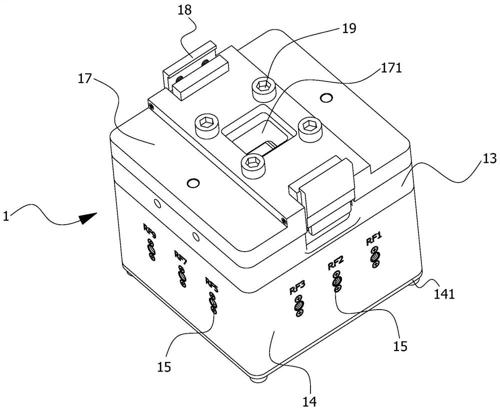
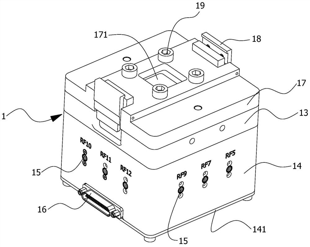
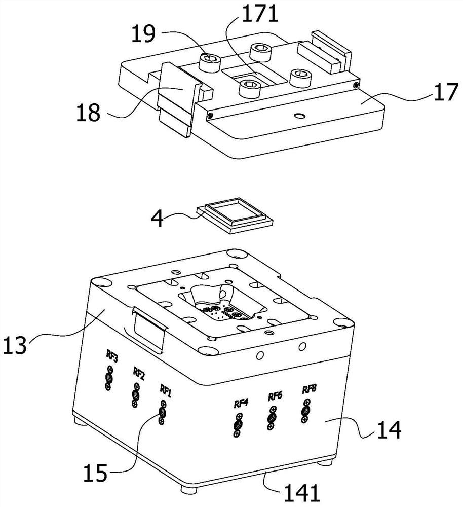
[0032] Such as Figure 1~4 As shown, a chip testing device is used to test the measured object 4 containing a radio frequency microwave signal port 41. The chip testing device includes a test base 1, and the test base 1 is embedded with a radio frequency microwave detection body 2, The radio-frequency microwave detection body 2 includes a conductor 21, and a radio-frequency elastic probe 22 wrapped with an insulating sheath 23 is inserted in the upper part of the conductor 21, and a plurality of auxiliary grounding elastic probes 22 are provided around the outer circumference of the radio-frequency elastic probe 22. Probe ...


PUM


Abstract

The invention relates to a chip testing device, which comprises a testing base, a radio frequency microwave detection body is embedded in the testing base, the radio frequency microwave detection bodycomprises a conductor, a radio frequency elastic probe externally wrapped by an insulating sleeve is inserted into the upper portion in the conductor, and a plurality of auxiliary grounding elastic probes are arranged on the outer side of the radio frequency elastic probe in the circumferential direction in a surrounding mode. The upper end part of the radio frequency elastic probe is in contactwith a radio frequency microwave signal port of a tested object, the lower end part of the radio frequency elastic probe is conductively connected with a radio frequency inner conductor arranged at the middle part in the conductor, a radio frequency cable is inserted into the lower part in the conductor, and a central conductor in the radio frequency cable is conductively connected with the lowerend part of the radio frequency inner conductor. According to the radio frequency elastic probe, a fuzz button structure is adopted as a main transmission channel of a radio frequency microwave signal, meanwhile, a transmission channel of a coaxial structure is also formed in the portion, making contact with a tested object, of the radio frequency elastic probe, the impedance matching effect is well achieved by arranging a compensation structure so that reflection of the radio frequency microwave signal can be reduced, and high-frequency and large-current testing can be met.

Description

technical field [0001] The invention belongs to the technical field of semiconductor integrated circuits, in particular to a chip testing device. Background technique [0002] For communication equipment manufacturers, half of the reasons why products are abnormal on the client side are hardware problems, and among hardware problems, chip failure is the main problem. Analyzing the failure of the chip, finding out the cause and improving it is the most critical part of improving the quality of product hardware. IV test (i.e. current and voltage test) is the most important link in chip failure analysis. Through the test of each pin of the chip, it can point out the ideas and directions for subsequent failure analysis. When the chip is tested, it needs to be connected with the automatic test equipment through the test fixture. [0003] The main components of test sockets currently on the market include spring probes, probe holders, and other electronic connectors. There is a...

Claims


Application Information

Patent Timeline
Patent Type & Authority Applications(China)
IPC IPC(8): G01R31/28G01R1/04
CPCG01R1/0416G01R31/2851G01R31/2886
Inventor 吕淑起宋德柱罗维
Owner SHANGHAI AEROSPACE SCI & IND ELECTRIC APPLIANCE RES INST
Why Eureka
Try Eureka