Attenuation reduction structure for high frequency signal contact pads of circuit board
一种高频信号、连接垫的技术,应用在电气连接印刷元件、印刷电路、印刷电路等方向,能够解决缺少解决方法高频信号传送等问题,达到降低电容效应的效果
- Summary
- Abstract
- Description
- Claims
- Application Information
AI Technical Summary
Problems solved by technology
Method used
Image
Examples
Embodiment Construction
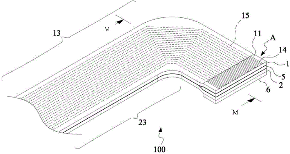
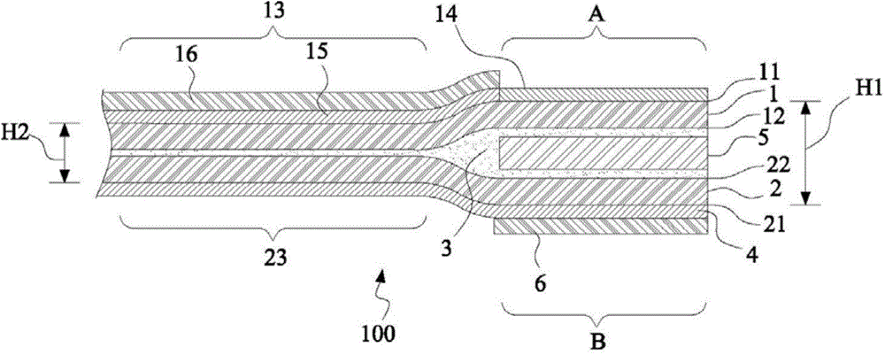
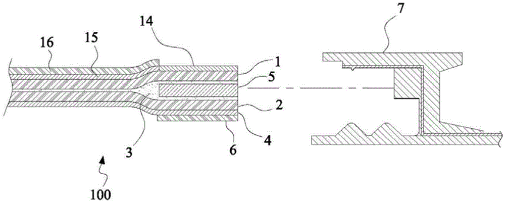
[0063] see figure 1 and figure 2 The circuit board 100 according to the first embodiment of the present invention has a circuit layout surface 11 and a ground wire layout surface 21, and a connection pad layout section A and a connection pad layout section A corresponding to the connection pad layout section A are provided on the circuit layout surface 11. Corresponding section B of . The structure of the circuit board 100 in this embodiment includes a first substrate 1, a second substrate 2, an adhesive layer 3, a ground layer 4, a plurality of high-frequency signal connection pads 14 and a plurality of high-frequency signal lines 15 .
[0064] The first substrate 1 has a circuit layout surface 11 and a first bonding surface 12, wherein the circuit layout surface 11 defines a connection pad layout section A and a first extension extending from the connection pad layout section A. Section 13.
[0065] A plurality of high-frequency signal connection pads 14 are arranged ad...
PUM
 Abstract
Description
Claims
Application Information


