A low-capacitance vertical-cavity surface-emitting laser and its manufacturing method

A vertical cavity surface emission and manufacturing method technology, applied in the field of vertical cavity surface emitting lasers and production, can solve the problems of poor MIS capacitance effect reduction effect, serious electrode capacitance effect, and deterioration of chip solderability, etc., to reduce MIS Effect of capacitive effect, reduction of dielectric constant, and improvement of solderability

Active Publication Date: 2022-03-18
泉州市三安光通讯科技有限公司
View PDF7 Cites 0 Cited by
  • Summary
  • Abstract
  • Description
  • Claims
  • Application Information

AI Technical Summary

Problems solved by technology

Due to the low defect density of N-type substrates, GaAs-based VCSELs generally use N-type substrates as substrates at present, and use the same-side electrode structure, and the capacitive effect of electrodes is very serious.
In order to reduce the electrode capacitance, the currently commonly used method is to insert a thick dielectric film insulating layer or an organic polymer layer under the electrode, and reduce the capacitance by increasing the thickness of the insulating medium. This process has a negative impact on the MIS capacitance effect formed between the electrode and the underlying structure. The reduction effect is not good, and the solderability of the chip is seriously deteriorated

Method used


Image

  • A low-capacitance vertical-cavity surface-emitting laser and its manufacturing method
  • A low-capacitance vertical-cavity surface-emitting laser and its manufacturing method
  • A low-capacitance vertical-cavity surface-emitting laser and its manufacturing method

Examples


Embodiment 1

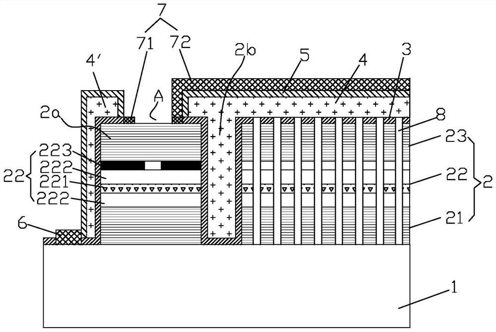
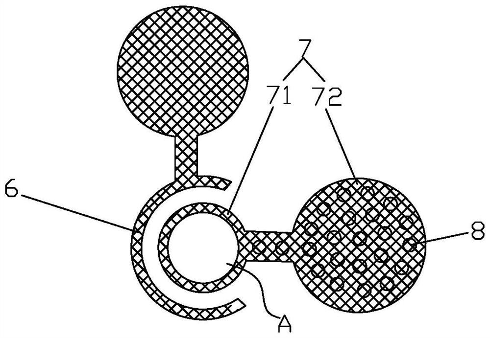
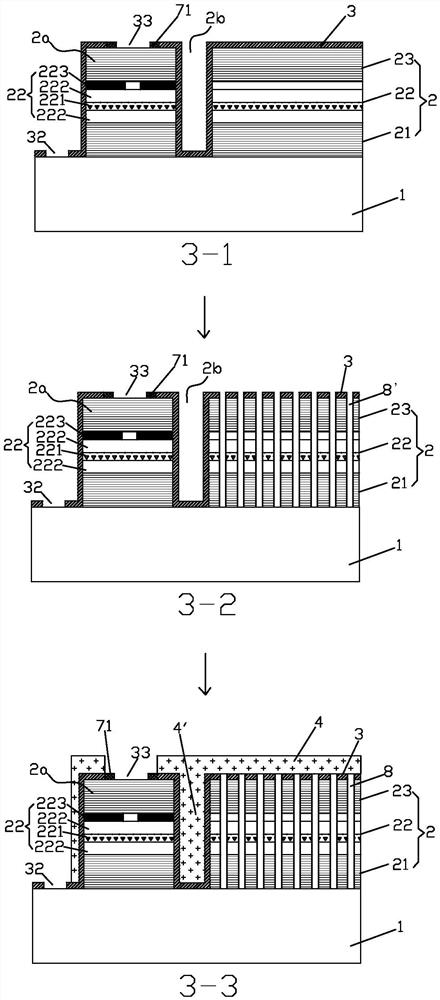
[0038]With the above structure, the first DBR 21 has a thickness of 5.14 μm and an equivalent dielectric constant of 11.59; the resonant cavity 22 has a thickness of 0.0.246 μm and an equivalent dielectric constant of 11.35; the second DBR 23 has a thickness of 3.19 μm and an equivalent The dielectric constant is 11.59; the thickness of the organic polymer layer 4 is 1 μm, and the dielectric constant is 2.25; the total thickness of the first dielectric layer 3 and the second dielectric layer 5 is 0.2 μm, and the dielectric constant is 3.8. The total area of ​​the air column 8 accounts for 50% of the coverage area of ​​the lead-out portion 72 , and the air column 8 penetrates the epitaxial layer 2 . It can be seen through calculation that the equivalent dielectric constant of the above structure is reduced by 44%, and thus the electrode capacitance can be reduced by more than 44%.

[0039] By setting the percentage of the total area of ​​different air columns to the coverage ar...


PUM

PropertyMeasurementUnit
diameteraaaaaaaaaa
thicknessaaaaaaaaaa
thicknessaaaaaaaaaa

Abstract

The invention discloses a low-capacitance vertical cavity surface emitting laser, which comprises a substrate, an epitaxial layer, a first electrode, a second electrode and an organic polymer layer, wherein the epitaxial layer forms a light-emitting area of ​​a device through insulation isolation, and the second electrode includes The ring part and the lead-out part, the ring part is arranged on the light-emitting area of ​​the device and the light outlet of the laser is formed inside, the lead-out part extends from the ring-shaped part to outside the light-emitting area of ​​the device, and the epitaxial layer outside the light-emitting area of ​​the device below the lead-out part is provided with A plurality of air columns extending downward, the organic polymer layer is arranged between the lead-out part and the epitaxial layer. The invention also discloses a manufacturing method of the above-mentioned laser. The present invention reduces the equivalent dielectric constant of the material under the second electrode by making a number of hole-like structures in the epitaxial layer under the second electrode and forming an air column, reduces the overall thickness and surface thickness difference, and improves the solderability of the chip. significantly improved.

Description

technical field [0001] The invention relates to the technical field of lasers, in particular to a low capacitance vertical cavity surface emitting laser and a manufacturing method. Background technique [0002] With the development of communication technology, the demand for optical chips used in data centers has increased dramatically. GaAs-based vertical-cavity surface-emitting lasers (VCSELs) have been widely used as a low-cost, high-performance light source for short-distance communication. At present, GaAs-based VCSEL products have transitioned from 10G to 25G. With the increase of transmission rate, VCSEL must have extremely low junction capacitance and additional capacitance. The junction capacitance is mainly achieved by reducing the area of ​​the PN junction. The additional capacitance mainly comes from the contribution of the electrode capacitance, so reducing the additional capacitance must reduce the contribution of the electrode capacitance. Due to the low d...

Claims


Application Information

Patent Timeline
Patent Type & Authority Patents(China)
IPC IPC(8): H01S5/183H01S5/042
CPCH01S5/183H01S5/18361H01S5/04254
Inventor 张江勇林科闯
Owner 泉州市三安光通讯科技有限公司
Why Eureka
Try Eureka