Connector structure and method of making the same

A manufacturing method and connector technology, applied in the direction of connection, fixed connection, electrical connection of printed components, etc., can solve problems affecting signal transmission performance and achieve the effect of reducing capacitance effect

Active Publication Date: 2018-07-13
UNIMICRON TECH CORP
View PDF5 Cites 0 Cited by
  • Summary
  • Abstract
  • Description
  • Claims
  • Application Information

AI Technical Summary

Problems solved by technology

When the connector structure 50 transmits signals through the terminals 58, the two conductor layers will generate a capacitive effect at the dielectric layer 57, thereby affecting the performance of signal transmission

Method used


Image

  • Connector structure and method of making the same
  • Connector structure and method of making the same
  • Connector structure and method of making the same

Examples


Embodiment Construction

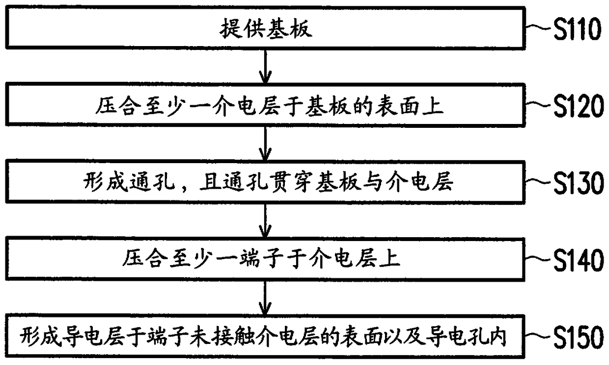
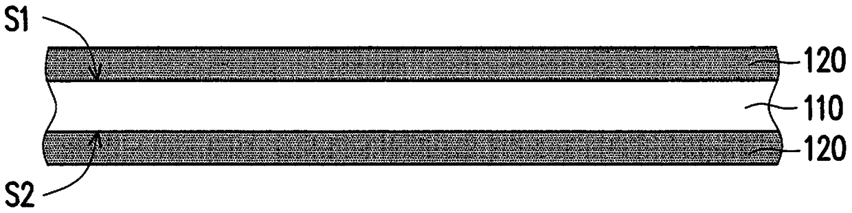
[0035] figure 2 It is a flow chart of making the connector structure of the embodiment of the present invention. Figure 3A to Figure 3D yes figure 2 Schematic cross-sectional illustration of the fabrication method of the connector structure. Please refer to figure 2 , in this embodiment, the manufacturing method of the connector structure 100 includes the following steps: In step S110 , a substrate 110 is provided. In step S120 , at least one dielectric layer 120 is laminated on the surface of the substrate 110 . In step S130 , a via hole 112 is formed, and the via hole 112 penetrates through the substrate 110 and the dielectric layer 120 . In step S140 , at least one terminal 130 is pressed on the dielectric layer 120 , and the terminal 130 is pressed on a side of the dielectric layer 120 that is locally adjacent to the through hole 112 . In step S150 , a conductive layer 140 is formed on the surface of the terminal 130 not in contact with the dielectric layer 120 an...


PUM


Abstract

The invention discloses a connector structure and a manufacture method thereof. The manufacture method comprises the following steps that a substrate is provided, at least one dielectric layer is formed on the surface of the substrate in a press fit mode, a through hole penetrates through the substrate and the dielectric layers, at least one terminal is formed on the dielectric layers in a press fit mode, the terminals are located on the sides, adjacent to the through hole, of the parts of the dielectric layers in a press fit mode, conducting layers are formed on the surfaces, making no contact with the dielectric layers, of the terminals and in the through hole, and the terminals and the through hole are electrically connected to form the conducting through hole. The invention also discloses the connector structure manufactured through the method.

Description

technical field [0001] The present invention relates to a connector structure, and more particularly, the present invention relates to a manufacturing method of the connector structure. Background technique [0002] In recent years, in order to increase the application of circuit boards, various types of connectors are manufactured on the circuit boards, so that the electronic devices equipped with the circuit boards have more application functions. Among them, some connectors can be directly fabricated on the circuit board during the production process of the circuit board. [0003] figure 1 is a schematic diagram of a known connector structure. Please refer to figure 1 , the manufacturing method of the connector structure 50 is to provide the substrate 52, and form a through hole on the substrate 52, and plate the upper and lower surfaces of the through hole and the part of the through hole on the substrate 52 to form a circuit layer 54 on the upper and lower surfaces o...

Claims


Application Information

Patent Timeline
Patent Type & Authority Patents(China)
IPC IPC(8): H05K1/11H05K3/40
CPCH01R12/51H01R43/00H05K1/116H05K1/119H05K2201/0394
Inventor 范智朋谢清河苏铃凯郑尹华
Owner UNIMICRON TECH CORP
Why Eureka
Try Eureka