A circuit layout structure

A technology of circuit layout and dielectric layer, which is applied in the field of special circuit layout structure, can solve the problems of inability to connect electrically, inability to expose metal contact plugs, etc., and achieve the effect of reducing the capacitive effect

Active Publication Date: 2017-04-12
UNITED MICROELECTRONICS CORP
View PDF4 Cites 0 Cited by
  • Summary
  • Abstract
  • Description
  • Claims
  • Application Information

AI Technical Summary

Problems solved by technology

Due to the static electricity generated by the electrostatic device, it is likely to induce the conductive metal mask 130 through the substrate 101, such as a titanium nitride mask, and induce the metal pattern 114 located in the scribe line 103 to form an unfavorable capacitance. , and then attract too much charged etching residue to accumulate in the bottom of the trench 121 in the chip region 102, and then the metal contact plug 111 under it cannot be exposed, and the electrical connection cannot be effectively formed.

Method used


Image

  • A circuit layout structure
  • A circuit layout structure
  • A circuit layout structure

Examples


Embodiment Construction

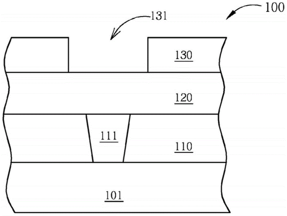
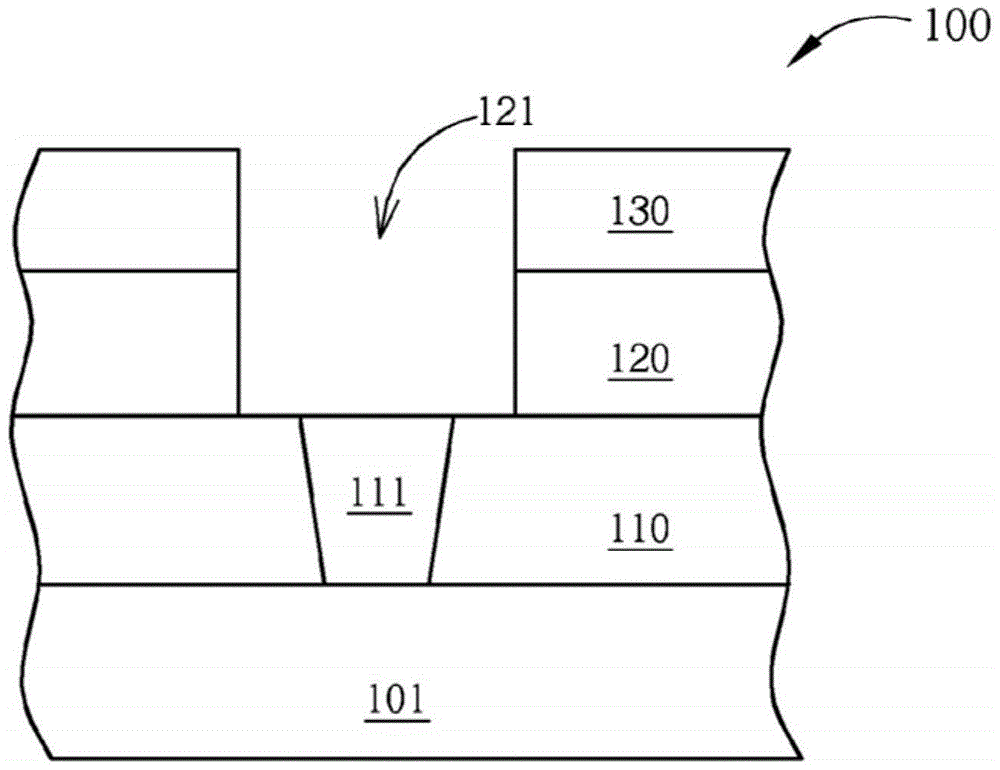
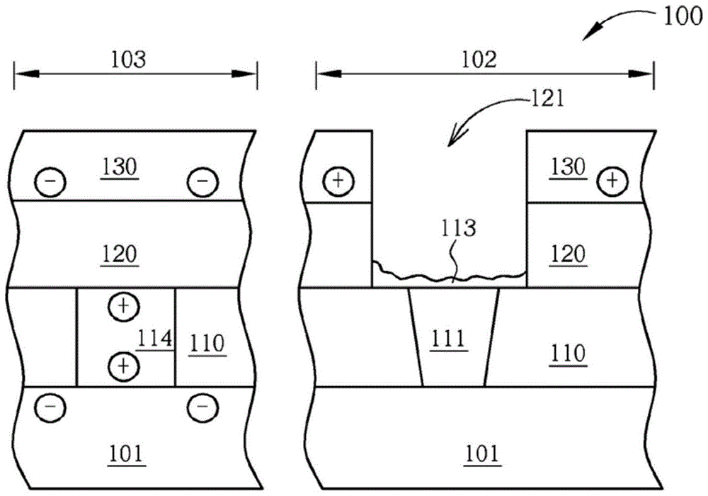
[0048] The present invention provides various novel circuit layout structures. In the circuit layout structure provided by the present invention, the metal mask and the metal pattern located in the scribe line can be properly isolated to reduce the charge induction between the metal mask and the metal pattern. Therefore, during the etching step, excessive etching residues are blocked in the trenches, hindering the etching process, and making it difficult to expose the underlying metal contact plugs. Especially when the metal mask is adjacent to the dicing line with the metal pattern, there will not be too much etching residue blocked in the groove of the inter-metal dielectric layer for the preparation of the metal interconnection, thus effectively avoiding the metal The problem that it is difficult to form an electrical connection between the interconnection wire and the underlying metal contact plug.

[0049] Figure 4A A cross-sectional view illustrating the first embodim...


PUM


Abstract

The invention discloses a circuit layout structure. The circuit layout structure comprises a metal interlayer dielectric layer and a metal pattern, wherein the metal interlayer dielectric layer surrounds a metal inner connecting wire; the metal pattern is positioned in a cutting path; the cutting path is adjacent to the metal interlayer dielectric layer and the metal inner connecting wire; and the metal inner connecting wire or the metal pattern is isolated properly so as to reduce capacitance effect.

Description

[0001] This application is a divisional application of an invention patent application with a filing date of November 23, 2009, an application number of 200910225937.8, and an invention title of "a circuit layout structure". technical field [0002] The invention relates to a circuit layout structure. In particular, the present invention relates to a special circuit layout structure. In these circuit layout structures, the metal interconnection surrounded by the inter-metal dielectric layer is properly isolated from the metal pattern in the scribe line, so as to reduce the undesirable capacitance effect. Background technique [0003] During the manufacture of semiconductor devices, etching processes are often used to create predetermined patterns in predetermined material layers. Figure 1-Figure 3 Illustrative of the process of using conventional etching procedures to create a predetermined pattern in a predetermined material layer in the known art. First, please refer to ...

Claims


Application Information

Patent Timeline
Patent Type & Authority Patents(China)
IPC IPC(8): H01L23/528
Inventor 蔡青龙白世杰刘山张瑜
Owner UNITED MICROELECTRONICS CORP
Why Eureka
Try Eureka