Semiconductor Switching Device with Different Local Cell Geometry

A semiconductor and device technology, applied in the field of semiconductor devices, can solve problems such as inhomogeneity, simultaneous operation of switchable units not guaranteed, and uneven switching

Active Publication Date: 2015-12-30
INFINEON TECH AUSTRIA AG
View PDF3 Cites 0 Cited by
  • Summary
  • Abstract
  • Description
  • Claims
  • Application Information

AI Technical Summary

Problems solved by technology

Furthermore, this non-uniform distribution of external switching signals across the chip area can prevent the switchable cells from switching simultaneously
Simultaneous operation of switchable units is therefore not guaranteed and non-uniform switching may occur

Method used


Image

  • Semiconductor Switching Device with Different Local Cell Geometry
  • Semiconductor Switching Device with Different Local Cell Geometry
  • Semiconductor Switching Device with Different Local Cell Geometry

Examples


Embodiment Construction

[0023] In the following detailed description, reference is made to the accompanying drawings which form a part hereof, and in which are shown specific embodiments in which the invention may be practiced. In this respect, terms such as "top", "bottom", "front", "rear", "front", "end", "landscape", " Directional terms such as "vertical". Because components of an embodiment may be positioned in a number of different orientations, directional terminology is used for purposes of illustration and is in no way limiting. It is to be understood that other embodiments may be utilized and structural or logical changes may be made without departing from the scope of the present invention. The following detailed description should therefore not be read in a limiting sense, and the scope of the invention is defined by the appended claims. The embodiments being described use specific language which should not be construed as limiting the scope of the appending claims.

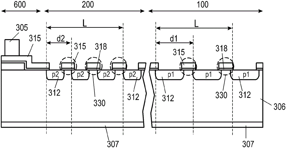
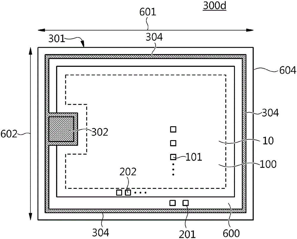
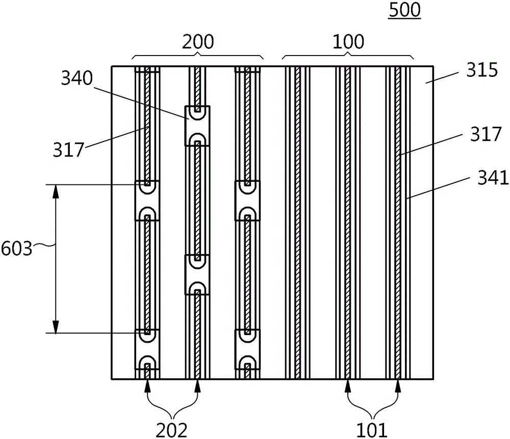
[0024] Reference w...


PUM


Abstract

A semiconductor device includes a semiconductor substrate having an outer rim, a plurality of switchable cells defining an active area, and an edge termination region arranged between the switchable cells defining the active area and the outer rim. Each of the switchable cells includes a body region, a gate electrode structure and a source region. A source metallization is in ohmic contact with the source regions of the switchable cells. A gate metallization is in ohmic contact with the gate electrode structures of the switchable cells. The active area defined by the switchable cells includes at least a first switchable region having a specific gate-drain capacitance which is different to a specific gate-drain capacitance of a second switchable region.

Description

technical field [0001] Embodiments described herein relate to semiconductor devices, and in particular to semiconductor switching devices, such as semiconductor power switches with different local cell geometries (and in particular locally different gate-drain capacitances). Furthermore, embodiments described herein relate to cell layouts of switchable cells located in an active area of ​​a semiconductor device. Background technique [0002] A semiconductor switching device with a large chip area is provided with a gate signal transmitter or gate runner structure, for example for passing an external switching signal provided by an external circuit to a gate arranged in the active area of ​​the semiconductor switching device. Gate pads, gate rings or gate fingers of the overall switchable cell. [0003] Cells located at or near the outer rim of the chip area (where gate metallization such as gate runner structures are provided) may receive external switching at a time before...

Claims


Application Information

Patent Timeline
Patent Type & Authority Applications(China)
IPC IPC(8): H01L29/06H01L21/336
CPCH01L29/0603H01L29/66477H01L29/41766H01L29/7811H01L29/0696H01L29/66712H01L29/7802H01L29/4238H01L2224/0603H01L29/7831H01L29/66484H01L21/823475H01L21/823481H01L27/11803
Inventor C.法赫曼E.贝西诺巴斯克斯
Owner INFINEON TECH AUSTRIA AG
Why Eureka
Try Eureka