Check patentability & draft patents in minutes with Patsnap Eureka AI!

VDMOS device manufacturing method and VDMOS device

A manufacturing method and device technology, applied in semiconductor/solid-state device manufacturing, semiconductor devices, electrical components, etc., can solve problems affecting the dynamic characteristics of VDMOS devices, and achieve the effect of solving dynamic characteristics and avoiding gate-to-drain capacitance

Active Publication Date: 2016-01-06
FOUNDER MICROELECTRONICS INT
View PDF4 Cites 5 Cited by
  • Summary
  • Abstract
  • Description
  • Claims
  • Application Information

AI Technical Summary

Problems solved by technology

[0003] The technical problem to be solved by the present invention is to provide a manufacturing method of a VDMOS device and a VDMOS device to solve the problem that the capacitance between the gate and drain in the structure of the planar VDMOS device in the prior art affects the dynamic characteristics of the VDMOS device

Method used


Image

  • VDMOS device manufacturing method and VDMOS device
  • VDMOS device manufacturing method and VDMOS device
  • VDMOS device manufacturing method and VDMOS device

Examples


Embodiment Construction

[0056] In order to make the technical problems, technical solutions and advantages to be solved by the present invention clearer, the following will describe in detail with reference to the drawings and specific embodiments.

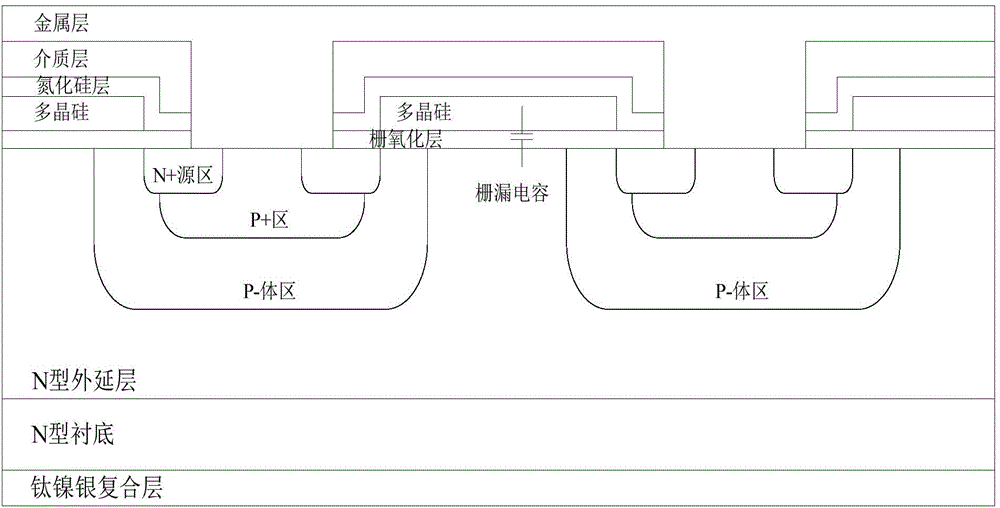
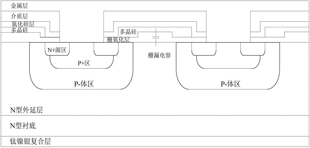
[0057] The present invention aims at the problem that the capacitance between the gate and the drain in the structure of the planar VDMOS device in the prior art affects the dynamic characteristics of the VDMOS device, and provides a method for manufacturing the VDMOS device, such as Figure 3 to Figure 11 shown, including the following steps:

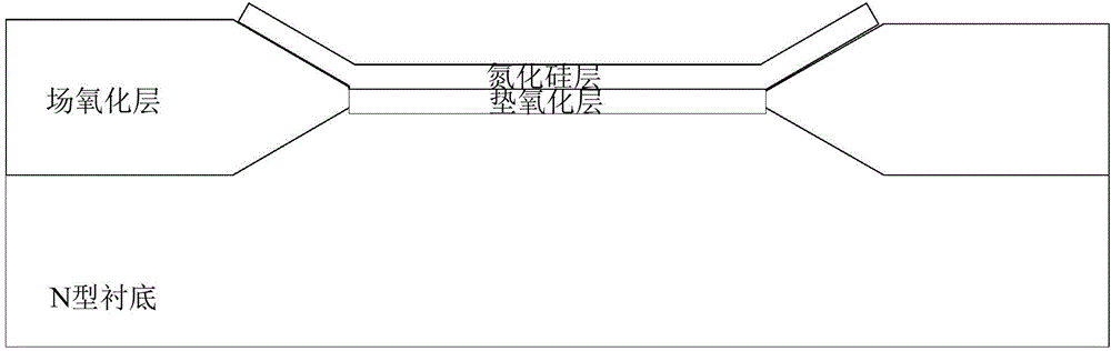
[0058] generating field oxide layers on opposite sides of the first surface of the N-type substrate;

[0059] forming a P-type body region between the field oxide layers on the first surface;

[0060] forming an N-type source region on the P-type body region;

[0061] Etching the field oxide layer to expose the P-type body region;

[0062] forming a gate oxide layer on the basis of the N-type source region;

[...


PUM

PropertyMeasurementUnit
Thicknessaaaaaaaaaa
Thicknessaaaaaaaaaa

Abstract

The invention provides a VDMOS device manufacturing method and a VDMOS device. The VDMOS device comprises an N type substrate, field oxides positioned at two opposite sides of a first surface of the N type substrate, a P type body region between the field oxides on the first surface, an N type source region positioned on the P type body region, a gate oxide positioned on the N type source region, an open polysilicon layer positioned on the gate oxide, a dielectric layer positioned on the field oxides, the polysilicon layer and the gate oxide, a first metal layer positioned on the dielectric layer and the P type body region, and a second metal layer positioned on the N type substrate and a second surface opposite to the first surface. The dielectric layer leads to the P type body region by etching, thereby forming a contact hole. The first metal layer forms poles of a grid electrode and a source electrode of the VDMOS device after being photoetching and etching. By the scheme provided by the invention, a gate-drain capacitor is omitted, and the problem that dynamic features are influenced by capacitance between the gate and the drain of a planar VDMOS device structure is solved.

Description

technical field [0001] The invention relates to the technical field of semiconductor chip manufacturing technology, in particular to a method for manufacturing a VDMOS device and the VDMOS device. Background technique [0002] In the structure of planar VDMOS, the capacitance between the gate and drain is mainly caused by the parasitic capacitance formed between the polysilicon gate / gate oxide layer / epitaxial layer (such as figure 1 Shown), this capacitor will affect the dynamic characteristics of VDMOS. In order to reduce this capacitance value, there are currently two main methods. The first is to increase the thickness of the gate oxide layer as a whole (such as figure 1 In the gate oxide layer), but this will affect other parameters of VDMOS, such as threshold voltage. The second approach is to locally increase the thickness of the gate oxide (eg figure 2 shown), this method can reduce the gate-to-drain capacitance to a certain extent, and can also avoid the influenc...

Claims


Application Information

Patent Timeline
IPC IPC(8): H01L21/336H01L29/78H01L29/06
Inventor 马万里
Owner FOUNDER MICROELECTRONICS INT
Features
  • R&D
  • Intellectual Property
  • Life Sciences
  • Materials
  • Tech Scout
  • Unparalleled Data Quality
  • Higher Quality Content
  • 60% Fewer Hallucinations
Learn More