
automatic PCB (Printed Circuit Board) scan image matching method and system

A scanning image, automatic matching technology, applied in the field of image scanning, can solve the problem that the PCB scanned image and the standard image cannot be completely aligned, and achieve the effect of accurate matching

Inactive Publication Date: 2016-01-13
SHENZHEN UNIV
View PDF6 Cites 13 Cited by
  • Summary
  • Abstract
  • Description
  • Claims
  • Application Information

AI Technical Summary

Problems solved by technology

[0003] The technical problem to be solved by the present invention is to provide an automatic matching method and system for PCB scan images, aiming to solve the problem that the PCB scan images to be tested and the standard images cannot be completely aligned

Method used


Image

  • automatic PCB (Printed Circuit Board) scan image matching method and system
  • automatic PCB (Printed Circuit Board) scan image matching method and system
  • automatic PCB (Printed Circuit Board) scan image matching method and system

Examples


Embodiment Construction

[0013] In order to make the object, technical solution and advantages of the present invention clearer, the present invention will be further described in detail below in conjunction with the accompanying drawings and embodiments. It should be understood that the specific embodiments described here are only used to explain the present invention, not to limit the present invention.

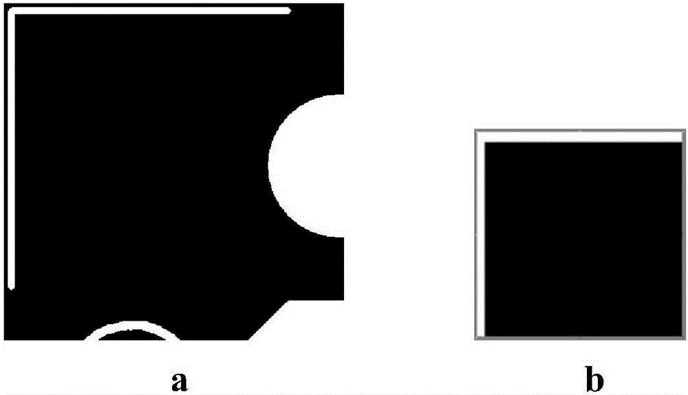
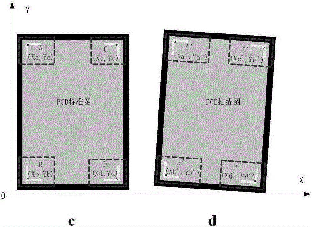
[0014] Before defect identification, the scanned image and the standard image need to be registered and precisely aligned. In the stage of circuit board process design and manufacturing, the designer usually sets a specific positioning mark on the PCB as the positioning standard for subsequent component welding and PCB cutting. For example, make an "L"-shaped mark on each of the four corners of the valid information of the PCB as a positioning Mark point, that is, a mark point. Each PCB has the same effective mark in the area framed by the "L" shape at the four corners information. Based on this f...


PUM


Abstract

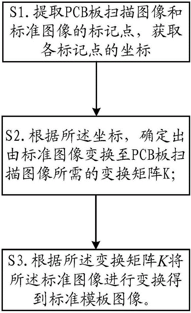
The present invention is applicable to the field of image scanning and provides an automatic PCB scan image matching method. The method comprises: step A, extracting marking points of a PCB scan image and a standard image, and acquiring coordinates of the marking points; step B, according to the coordinates of the marking points on the standard image and the coordinates of the marking points in the same positions of the PCB scan image, determining a transform matrix K for transforming the standard image into the PCB scan image; and step C, transforming the standard image according to the transform matrix K to obtain a standard template image. According to the automatic matching method and system provided by the present invention, a space transformation relationship between two images is found out by adopting a bilinear transform algorithm according to corresponding relationships among the coordinates of the similar feature points of the PCB scan image and the corresponding standard image, thereby acquiring a standard image with the same size as the scan image for subsequent defect comparison; and no manual interference is required, matching points can be automatically found out and calculated, the obtained scan image is substantially not distorted, and the matching is relatively precise, so that a foundation is laid for subsequent defect identification.

Description

technical field [0001] The invention belongs to the field of image scanning, and in particular relates to an automatic matching method and system for PCB scanning images. Background technique [0002] When using the reference comparison method to detect defects on a bare PCB, it is required that the scanned image of the PCB to be tested and the standard image must be completely aligned in space, otherwise many false positives will easily occur. However, due to factors such as edge process errors of the PCB bare board to be tested, workbench and camera shake, etc., there are differences in spatial positions between the collected and spliced ​​scanned images of the PCB to be tested and the standard images, and they cannot be completely aligned. Contents of the invention [0003] The technical problem to be solved by the present invention is to provide an automatic matching method and system for PCB scan images, aiming to solve the problem that the PCB scan images to be teste...

Claims


Application Information

Patent Timeline
Patent Type & Authority Applications(China)
IPC IPC(8): G06T7/00
CPCG06T7/001G06T2207/30141
Inventor 程涛冯平孙高磊徐刚彭小波
Owner SHENZHEN UNIV
Learn More