an electronic device

A technology of electronic devices and potentiometers, applied in coupling devices, circuits, discharge lamps, etc., can solve the problems of inconvenience to carry, thick thickness of the whole machine, and negative impact on the user's portable experience, so as to increase the beauty, the thickness, and improve the portability. sexual effect

Active Publication Date: 2018-01-23
GUANGDONG OPPO MOBILE TELECOMM CORP LTD
View PDF4 Cites 0 Cited by
  • Summary
  • Abstract
  • Description
  • Claims
  • Application Information

AI Technical Summary

Problems solved by technology

[0002] At present, the stacking method used by portable devices with potentiometers is to insert the potentiometers into the main board of the whole machine along the lead-out direction of the pins, and insert the pins of the potentiometers into the main board through the expansion slot of the main board, and the potential Because the potentiometer has pins, the size in the height direction is much larger than the size in the width direction. If the potentiometer pins are added, the thickness of the whole machine will become very thick. This stacking method makes the overall size of the portable device larger. Have a great negative impact on the user's portable experience
[0003] Specifically, see Figure 1a as well as Figure 1b , Figure 1a is the front view of the electronic device in the prior art, Figure 1b for Figure 1a The side view of the electronic device shown, wherein the electronic device 1 includes the front side 11 of the main board, the side 12 of the main board and a potentiometer 13, and the potentiometer 13 includes pins 131. In the prior art, the pins of the potentiometer are placed along the pins The lead-out direction is inserted into the expansion slot on the front of the motherboard. The pins of the potentiometer are perpendicular to the front of the motherboard. When calculating the thickness of the motherboard from the side of the motherboard, the thickness of the motherboard with the potentiometer becomes very thick, making the portable device The overall size is large, not easy to carry

Method used


Image

  • an electronic device
  • an electronic device
  • an electronic device

Examples


Embodiment Construction

[0020] The following will clearly and completely describe the technical solutions in the embodiments of the present invention with reference to the accompanying drawings in the embodiments of the present invention. Obviously, the described embodiments are only some, not all, embodiments of the present invention. Based on the embodiments of the present invention, all other embodiments obtained by persons of ordinary skill in the art without creative efforts fall within the protection scope of the present invention.

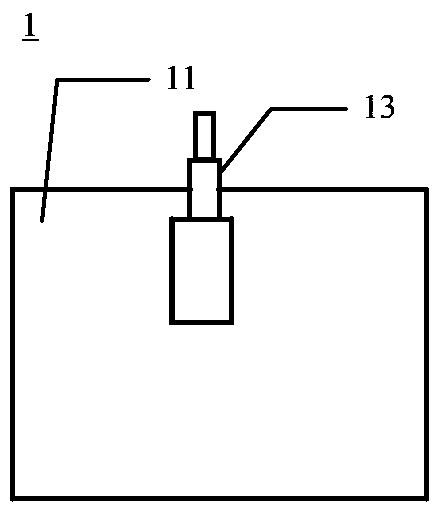
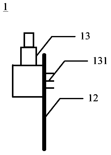
[0021] The electronic device of the embodiment of the present invention uses the main board and the potentiometer to make the thickness of the main board with the potentiometer thinner, improve the portability of the main board, and increase the delicacy of the appearance of the main board.

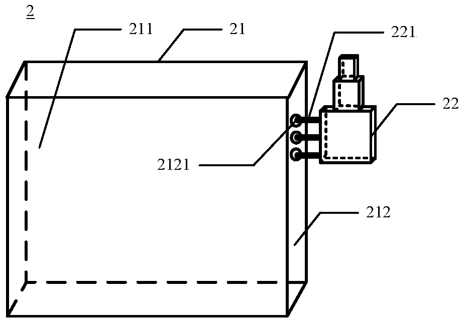
[0022] see figure 2 , is a schematic structural diagram of an electronic device provided by an embodiment of the present invention. Such as figure 2 As shown, the electron...


PUM


Abstract

The embodiment of the present invention discloses an electronic device, comprising: a main board and a potentiometer, the main board includes a front and a side, the front is adjacent to and perpendicular to the side, and circuits and electronic components are arranged on the front, the The potentiometer has at least one pin, the side is provided with a socket corresponding to the pin, and the pin of the potentiometer is inserted into the socket on the side. By adopting the embodiment of the present invention, the thickness of the main board installed with the potentiometer can be made thinner, the portability of the main board is improved, and the appearance of the main board is more exquisite.

Description

technical field [0001] The invention relates to the field of electronic equipment, in particular to an electronic device. Background technique [0002] At present, the stacking method used by portable devices with potentiometers is to insert the potentiometers into the main board of the whole machine along the lead-out direction of the pins, and insert the pins of the potentiometers into the main board through the expansion slot of the main board, and the potential Because the potentiometer has pins, the size in the height direction is much larger than the size in the width direction. If the potentiometer pins are added, the thickness of the whole machine will become very thick. This stacking method makes the overall size of the portable device larger. It has a great negative impact on the user's portable experience. [0003] Specifically, see Figure 1a as well as Figure 1b , Figure 1a is a front view of an electronic device in the prior art, Figure 1b for Figure 1a ...

Claims


Application Information

Patent Timeline
Patent Type & Authority Patents(China)
IPC IPC(8): H01R33/00H01R12/59H05K1/02
Inventor 邱泽朔
Owner GUANGDONG OPPO MOBILE TELECOMM CORP LTD
Why Eureka
Try Eureka