Supercharge Your Innovation With Domain-Expert AI Agents!

Wafer scheduling method and system

A dispatching method and dispatching system technology, applied in electrical components, conveyor objects, transportation and packaging, etc., can solve problems such as ineffective utilization, low transmission efficiency, and reduced transmission efficiency, so as to reduce waiting time and improve dispatching. Efficiency, the effect of improving utilization

Active Publication Date: 2018-11-06
BEIJING NAURA MICROELECTRONICS EQUIP CO LTD
View PDF8 Cites 0 Cited by
  • Summary
  • Abstract
  • Description
  • Claims
  • Application Information

AI Technical Summary

Problems solved by technology

[0004] For the above method, during the calibration process of the wafer, the manipulator is in a waiting state and cannot be effectively utilized, resulting in low transmission efficiency; in addition, the manipulator is also waiting during the process of the process module, which further reduces the transmission efficiency

Method used


Image

  • Wafer scheduling method and system
  • Wafer scheduling method and system
  • Wafer scheduling method and system

Examples


Embodiment Construction

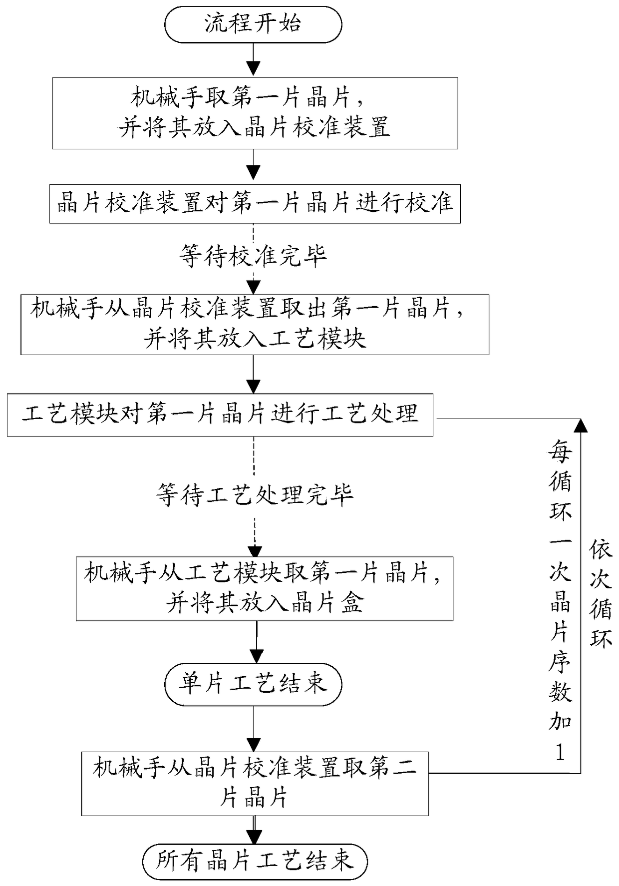
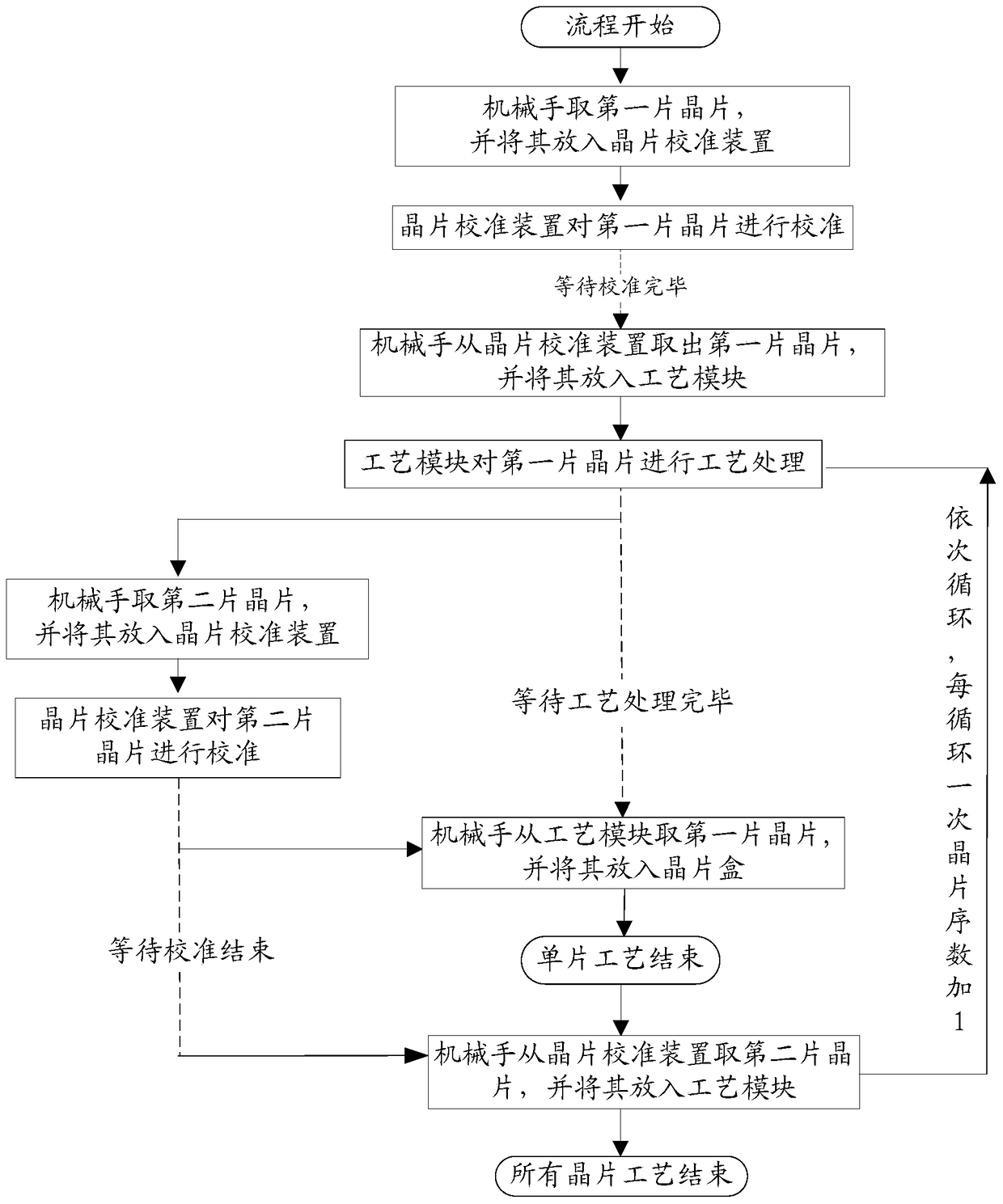
[0037] The specific implementation manners of the wafer scheduling method and system in the embodiments of the present invention will be described below with reference to the accompanying drawings.

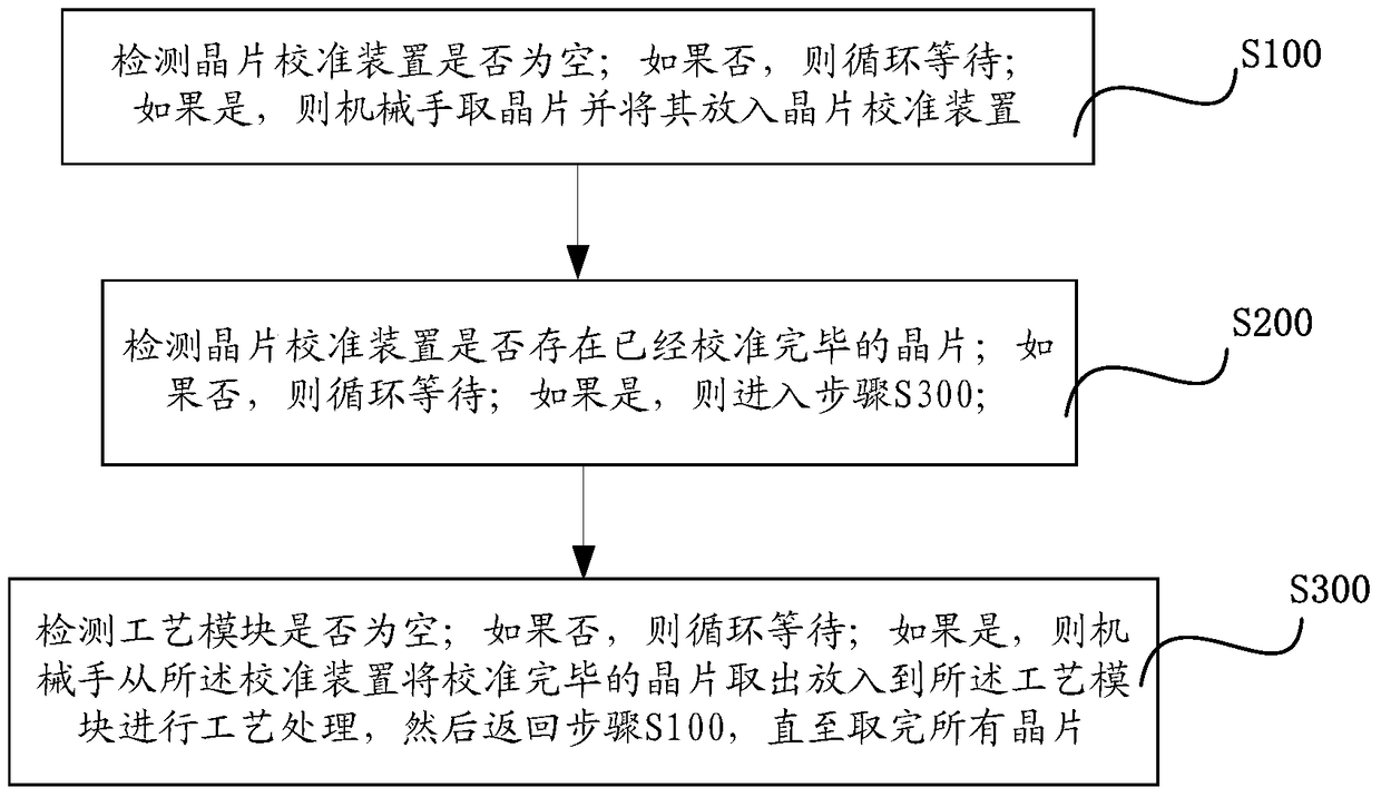
[0038] refer to figure 2 , the invention provides a method for scheduling wafers, comprising the following steps:

[0039] S100: Detect whether the wafer alignment device is empty; if not, enter step S200; if yes, the manipulator obtains the wafer and puts it into the wafer alignment device for calibration;

[0040] When the wafer calibration device is not empty, it means that there is a wafer in the wafer calibration device. At this time, enter step S200 to detect whether the calibration of the wafer in the calibration device is completed; when it is empty in the wafer calibration device, it means that there is no wafer in the wafer calibration device. , at this time, the manipulator is required to obtain the wafer and put it into the calibration device for calibration.

[004...


PUM


Abstract

The invention discloses a wafer scheduling method and system. The method comprises the following steps: S100) detecting whether a wafer calibration device is empty, if not, carrying out circular waiting, and if so, a mechanical arm getting a wafer and placing the wafer to the wafer calibration device for calibration; S200) detecting whether the wafer calibration device has the calibrated wafer, if not, carrying out circular waiting, and if so, entering the step S300); and S300) detecting whether a process module is empty, if not, carrying out circular waiting, and if so, the mechanical arm taking the calibrated wafer out of the calibration device and placing the wafer to the process module for processing, and then, returning to the step S100) until all the wafers are taken out. The wafer scheduling method and system improve utilization rate of the mechanical arm and scheduling efficiency of the wafers effectively.

Description

technical field [0001] The invention relates to a semiconductor preparation process, in particular to a wafer scheduling method and system. Background technique [0002] In the semiconductor manufacturing process, the wafer or substrate to be processed needs to be gradually transferred from the atmospheric environment to the process chamber for process processing. A wafer transfer system is usually used to transfer the wafer to the process chamber, and the system includes a transfer module and a control module. Among them, the transmission module includes a cassette loading device, a manipulator, a wafer alignment device and a process module; the functions of each part are as follows: the cassette loading device is used to load the cassette, the manipulator is used to transfer the wafer, and the wafer alignment device is used to calibrate the center of the wafer. , the process module is used to perform related process processing on the wafer. The control module is used to ...

Claims


Application Information

Patent Timeline
Patent Type & Authority Patents(China)
IPC IPC(8): H01L21/67H01L21/677
Inventor 魏晓
Owner BEIJING NAURA MICROELECTRONICS EQUIP CO LTD
Features
  • R&D
  • Intellectual Property
  • Life Sciences
  • Materials
  • Tech Scout
  • Unparalleled Data Quality
  • Higher Quality Content
  • 60% Fewer Hallucinations
Learn More