
Semiconductor wafer teaching jig

A semiconductor and wafer technology, applied in the field of semiconductor wafer teaching fixtures, can solve the problems of difficulty in clearly confirming whether the finger arm is accurately grasping the wafer, normal insertion, installation and extraction, inconvenient, accurate measurement and correction, etc.

Active Publication Date: 2017-11-14
丁炳铁
View PDF6 Cites 0 Cited by
  • Summary
  • Abstract
  • Description
  • Claims
  • Application Information

AI Technical Summary

Problems solved by technology

[0005] However, the original purpose of the carrier is to store and install wafers on the semiconductor manufacturing line for supply and transfer. However, if the above-mentioned carrier is used for teaching, it is difficult to clearly confirm whether the finger arm is accurately grasping the chip and inserting it normally during the teaching operation. Whether the mounting and extraction, or the operational relationship between the finger arm and the wafer is accurate
[0006] That is, it is difficult and inconvenient to accurately measure and correct the height, front progress, level, center, inclination, and position of the arm. Therefore, after setting up the equipment, it is necessary to perform teaching again at startup

Method used


Image

  • Semiconductor wafer teaching jig
  • Semiconductor wafer teaching jig
  • Semiconductor wafer teaching jig

Examples


Embodiment Construction

[0045] Below, the embodiments of the present invention will be described in detail with reference to the accompanying drawings.

[0046] The terms defined in the process of explaining the present invention are defined in consideration of the functions in the present invention, and cannot be regarded as limiting the technical constitution of the present invention.

[0047] The present invention can be variously modified and can have various embodiments, and in the following, the aspects will be described in detail. However, the present invention is not limited to a specific embodiment, and all modifications, equivalents, and substitutions belonging to the spirit and technical scope of the present invention are included.

[0048] In addition, the size and thickness of elements in each drawing are exaggerated or simplified to facilitate understanding, but the present invention is not limited to these drawings.

[0049] The terms used in the present application are used to illust...


PUM


Abstract

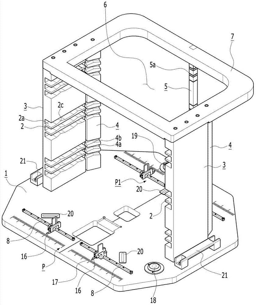
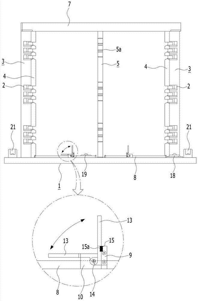
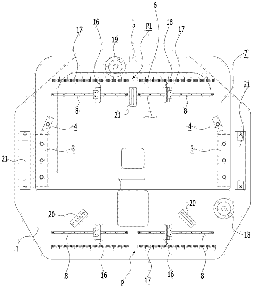
The present invention relates to a teaching jig for a semiconductor wafer mounted with a semiconductor wafer carrier to reteach when a damage, breakdown, or an error of an index arm extracting a wafer from a loading table, and when preventive maintenance (PM) occurs. The teaching jig comprises holder shafts, stopper shafts, a scale strip, a framework upper plate and first and second position measuring devices. The holder shafts are vertically arranged on two sides of a support plate and multiple holder grooves in which the semiconductor wafer can be inserted are formed on the holder shafts. The stopper shafts are vertically arranged on two side parts of the rear of the holder shafts and fix the semiconductor wafer according to the position. The scale strip is vertically arranged in the center of the rear of the holder shafts on two sides and scales for confirming the position of the semiconductor wafer are carved. The framework upper plate is fixedly arranged on the upper parts of the holder shafts, the stopper shafts and the scale strip. The first and second position measuring devices are arranged on front and back sides of the holder shafts.

Description

technical field [0001] The present invention relates to the case where the index arm (Index Arm) used to pick up the wafer (Wafer) is damaged or fails or is wrong in the loading table where the semiconductor wafer handler is installed in the semiconductor manufacturing line, or PM (Preventive Maintenance, in case of occurrence) Before a sudden failure, the operation behavior of stopping the equipment for pre-inspection and repair), etc. before the normal manufacturing process is started, the semiconductor wafer teaching jig for teaching (Teaching) for testing is especially involved in manufacturing for resetting the finger arm, etc. When the equipment is used for teaching, the position measurement and correction of the finger arm can be accurately and easily completed. At the same time, it is easy to confirm whether the finger arm is accurately grasping the chip and whether the chip is accurately inserted, installed and extracted through the finger arm. (Teaching) is a semicon...

Claims


Application Information

Patent Timeline
Patent Type & Authority Patents(China)
IPC IPC(8): G09B19/00
CPCB65D85/38H01L21/67778H01L21/68
Inventor 丁炳铁
Owner 丁炳铁
Learn More