Three-dimensional semiconductor device and manufacture method thereof

A device manufacturing method and semiconductor technology, which are applied to semiconductor devices, electric solid state devices, electrical components, etc., can solve the problems of easy breakdown of gate dielectrics, sharp corners of L-type transistors, and deterioration of reliability, and achieve suppression of local electric fields. Enhanced effect, improved reliability effect

Active Publication Date: 2016-03-02
INST OF MICROELECTRONICS CHINESE ACAD OF SCI
View PDF3 Cites 39 Cited by
  • Summary
  • Abstract
  • Description
  • Claims
  • Application Information

AI Technical Summary

Problems solved by technology

At this time, this non-90-degree etching will cause serious sharp corner problems in the L-type transistor. There will be a local strong electric field in this area, which will make the gate dielectric very prone to breakdown, thereby deteriorating reliability.

Method used


Image

  • Three-dimensional semiconductor device and manufacture method thereof
  • Three-dimensional semiconductor device and manufacture method thereof
  • Three-dimensional semiconductor device and manufacture method thereof

Examples


Embodiment Construction

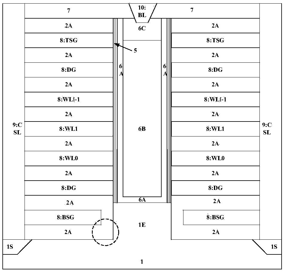
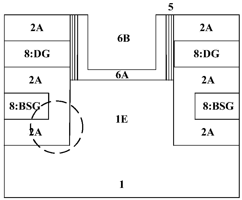
[0021] The features and technical effects of the technical solution of the present invention will be described in detail below with reference to the accompanying drawings and in conjunction with schematic embodiments, disclosing a semiconductor storage device and its manufacturing method that suppresses the local electric field enhancement effect and makes the electric field of the gate dielectric of the bottom transistor uniformly distributed . It should be pointed out that similar reference numerals represent similar structures, and the terms "first", "second", "upper", "lower" and the like used in this application can be used to modify various device structures or manufacturing processes . These modifications do not imply spatial, sequential or hierarchical relationships of the modified device structures or fabrication processes unless specifically stated.

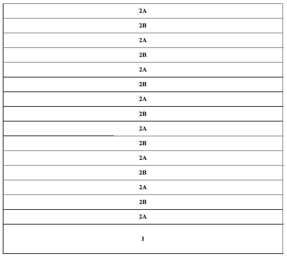
[0022] Such as Figure 2A As shown, an insulating layer stack 2 composed of a plurality of alternately stacked firs...


PUM


Abstract

Provided is a three-dimensional semiconductor device which comprises multiple storage units. Each storage unit comprises a channel layer stack, multiple insulated layers, multiple gate conductive layers, a gate dielectric layer, a drain, and a source. The channel layer stack is distributed along the direction vertical to the surface of a substrate. The multiple insulated layers and the multiple gate conductive layers are stacked alternately along the sidewall of the channel layer stack. The gate dielectric layer is arranged between the multiple gate conductive layers and the sidewall of the channel layer stack. The drain is arranged on the top of the channel layer stack. The source is arranged in the substrate between two adjacent storage units of the multiple storage units. The lowest insulated layer is provided with an obtuse or rounded corner portion. According to the three-dimensional semiconductor device and a manufacture method thereof, the closed angle of a transistor on the bottom is made obtuse or rounded in order to suppress a local electric field enhancement effect so that a gate dielectric electric field of the transistor on the bottom is uniformly distributed and reliability is improved.

Description

technical field [0001] The invention relates to a semiconductor device and a manufacturing method thereof, in particular to a three-dimensional semiconductor storage device and a manufacturing method thereof. Background technique [0002] In order to improve the density of memory devices, the industry has made extensive efforts to develop methods of reducing the size of two-dimensionally arranged memory cells. As the size of memory cells in two-dimensional (2D) memory devices continues to shrink, signal collisions and interference can increase significantly, making it difficult to perform multi-level cell (MLC) operations. In order to overcome the limitations of 2D memory devices, the industry has developed memory devices with a three-dimensional (3D) structure to increase integration density by three-dimensionally arranging memory cells on a substrate. [0003] Specifically, such as Figure 1A As shown, a multi-layer stack structure (for example, multiple ONO structures al...

Claims


Application Information

Patent Timeline
Patent Type & Authority Applications(China)
IPC IPC(8): H01L27/115H01L29/10H01L29/423
CPCH01L29/1033H01L29/4234H01L29/42364H10B43/20
Inventor 霍宗亮叶甜春
Owner INST OF MICROELECTRONICS CHINESE ACAD OF SCI
Why Eureka
Try Eureka