
Single-layer mutual-capacitance touch panel

A mutual-capacitance touch, single-layer technology, applied in electrical digital data processing, instruments, data processing input/output process, etc., can solve the problem of reducing user experience, unfavorable technology development, increasing production cost and operating power and other problems to achieve the effect of improving the touch effect, solving the suspension problem, and improving the user experience.

Inactive Publication Date: 2016-04-20
SHENZHEN YAMILA ELECTRONICS TECH CO LTD
View PDF5 Cites 4 Cited by
  • Summary
  • Abstract
  • Description
  • Claims
  • Application Information

AI Technical Summary

Problems solved by technology

[0004] With the rapid development of the touchpad, there have been some unacceptable problems, such as the floating problem of the touchpad, when the finger is close to the touchpad, multiple touch points are generated, which affects The normal touch function reduces the user experience. The conventional solution is to increase the coupling capacitance between the driving and sensing electrodes. In this case, the production cost and operating power will be increased, which is not conducive to normal technological development. It is the normal development direction of the touch panel to reduce the inherent capacitance between the finger and the sensing and driving without affecting the mutual capacitance between the electrodes, and finally realize normal touch without generating multiple touch points. Based on this, this field The technicians have carried out a lot of research and development work, and have also achieved outstanding results

Method used


Image

  • Single-layer mutual-capacitance touch panel
  • Single-layer mutual-capacitance touch panel
  • Single-layer mutual-capacitance touch panel

Examples


Embodiment Construction

[0025] In order to make the object, technical solution and advantages of the present invention clearer, the present invention will be further described in detail below in conjunction with the accompanying drawings and embodiments. It should be understood that the specific embodiments described here are only used to explain the present invention, not to limit the present invention.

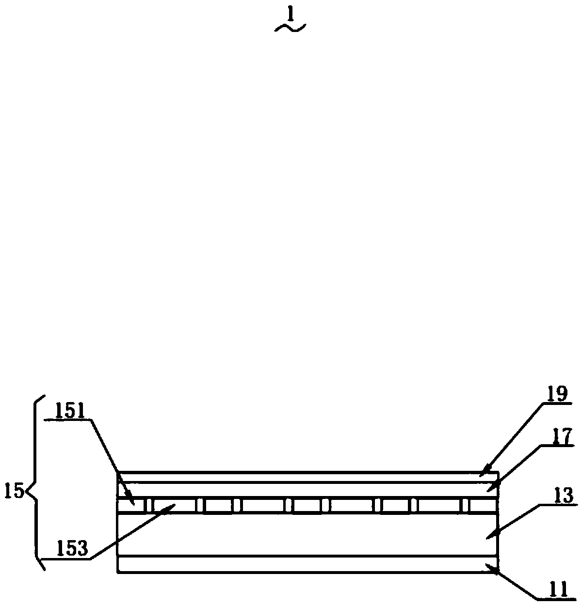
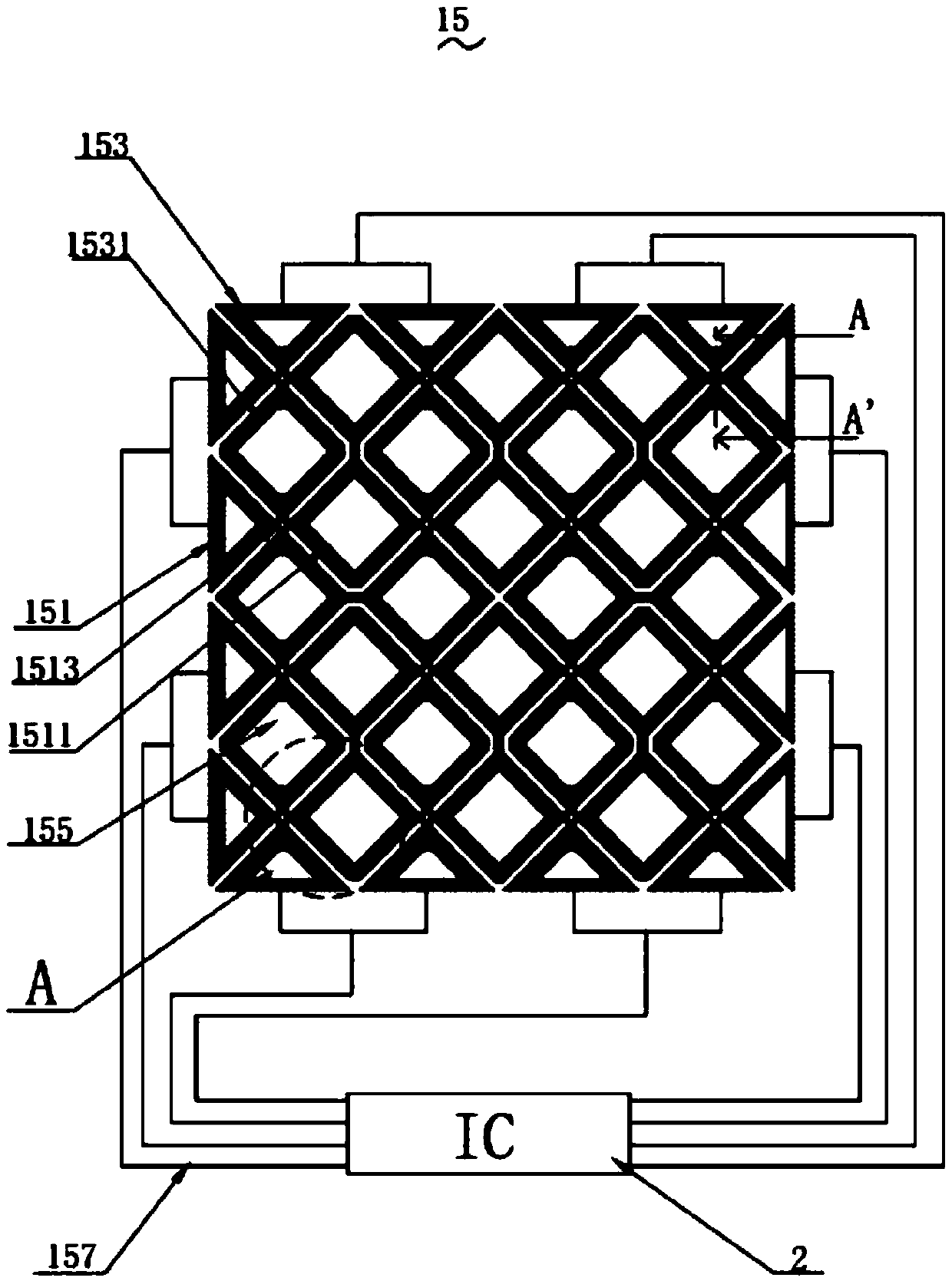
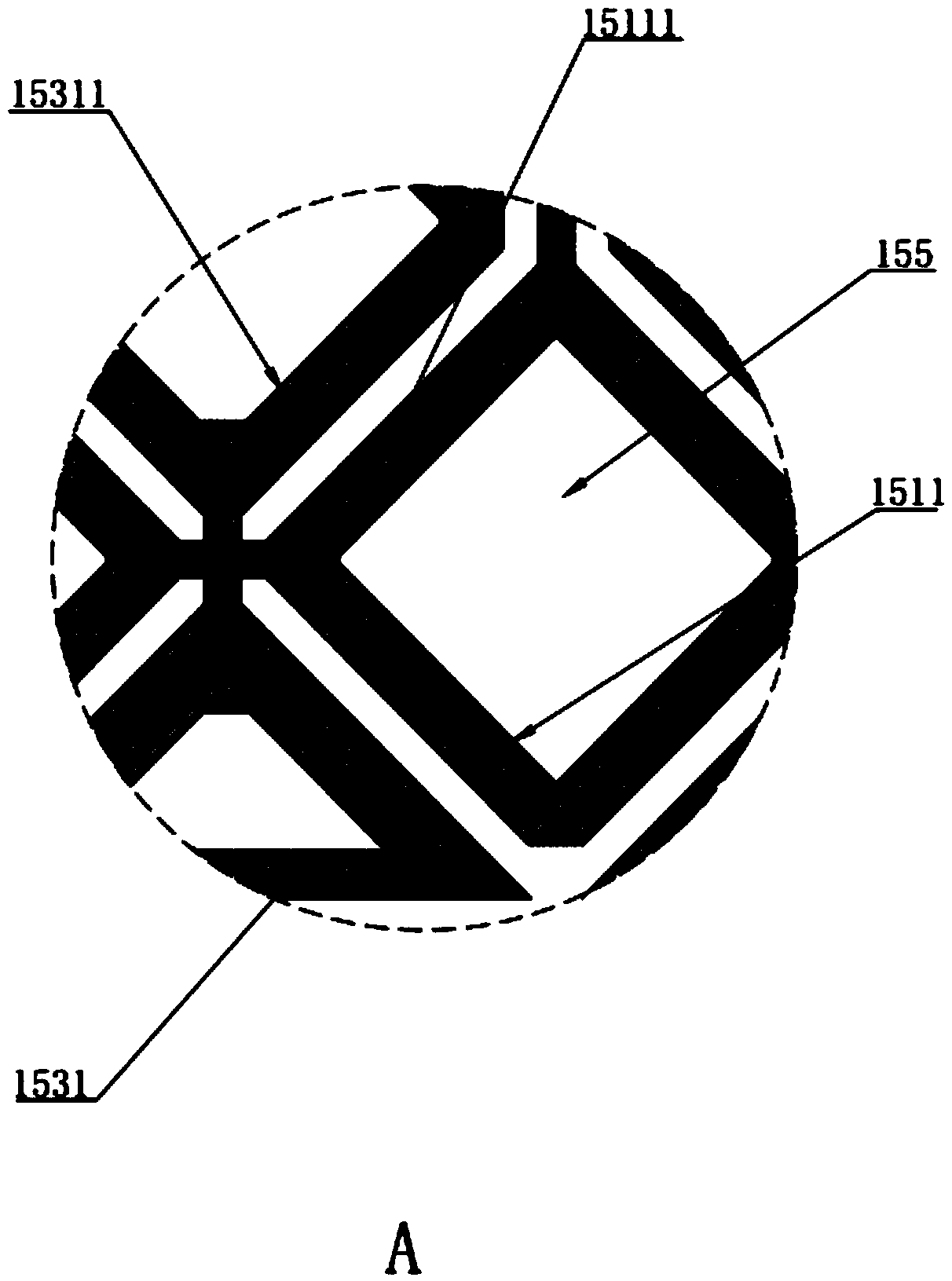
[0026] see figure 1 and figure 2 The single-layer mutual capacitance touch panel 1 of the present invention includes a substrate 13, a touch electrode layer 15, a first insulating layer 17 and a second insulating layer 11, and the touch electrode layer 15 includes at least two first direction touch electrodes 151 and At least two second direction touch electrodes 153, the first direction touch electrodes 151 and the second direction touch electrodes 153 are interlaced and arranged on the same surface of the substrate 13, the first direction touch electrodes 151 include a plurality of first The d...


PUM


Abstract

The invention provides a single-layer mutual-capacitance touch panel which comprises a substrate, first-direction touch electrodes and second-direction touch electrodes. The first-direction touch electrodes and the second-direction touch electrodes intersect with one another and are arranged on the surface of the substrate, each first-direction touch electrode comprises a plurality of first-direction touch electrode units, each second-direction touch electrode comprises a plurality of second-direction touch electrode units, the first-direction touch electrode units and the second-direction touch electrode units are provided with hollow-out regions, input ends of at least two adjacent first-direction touch electrodes or input ends of at least two adjacent second-direction electrodes are connected with each other, output ends of at least two adjacent first-direction touch electrodes or output ends of at least two adjacent second-direction touch electrodes are connected with each other, and each of the input ends and the output ends is connected with a chip by an electrode connecting wire. The single-layer mutual-capacitance touch panel has the advantages that the problem of floating can be effectively solved by the aid of the single-layer mutual-capacitance touch panel, and the single-layer mutual-capacitance touch panel is simple in structure, is integrally lightened and thinned and has good touch hand feel.

Description

[technical field] [0001] The invention relates to a touch panel, in particular to a single-layer mutual-capacitance touch panel with high touch accuracy and better solution to the levitation problem. [Background technique] [0002] The technology development of the touch panel is very diverse. At present, the more common technologies include resistive, capacitive and optical. Among them, the capacitive touch panel has high accuracy, multi-touch, high durability and high touch control. Resolution and other characteristics have become the mainstream touch technology used in mid-to-high-end consumer electronics products. [0003] The operation principle of the capacitive touch panel is to use the sensing electrodes to detect the capacitance change of the touch point, and use the connecting wires connecting the electrodes in different directions to transmit the signal back to complete the positioning. In recent years, with the touch sensing With the rapid development of technol...

Claims


Application Information

Patent Timeline
Patent Type & Authority Applications(China)
IPC IPC(8): G06F3/0354
CPCG06F3/03547
Inventor 陈威纪海鹏吴丽娟
Owner SHENZHEN YAMILA ELECTRONICS TECH CO LTD
Learn More