An OLED panel and a display device

A panel and thin film packaging technology, applied in electrical components, diodes, electrical solid devices, etc., can solve problems such as unfavorable outdoor visual functions, achieve outdoor visual functions, increase the brightness attenuation angle of a large viewing angle, and reduce the thickness.

Active Publication Date: 2018-12-11
BOE TECH GRP CO LTD
View PDF2 Cites 12 Cited by
  • Summary
  • Abstract
  • Description
  • Claims
  • Application Information

AI Technical Summary

Problems solved by technology

[0003] However, after the POL is replaced by the color film, the transmittance of the black matrix adjacent to the color film is basically 0, so the light emitted by the OLED can only pass through the color film
In order to increase the brightness attenuation angle of large viewing angles, it is necessary to increase the aperture ratio of the color filter. However, with the increase of the aperture ratio of the color filter, the reflectivity of the OLED panel also increases, which is not conducive to the realization of outdoor visual functions.

Method used


Image

  • An OLED panel and a display device
  • An OLED panel and a display device
  • An OLED panel and a display device

Examples


no. 1 example

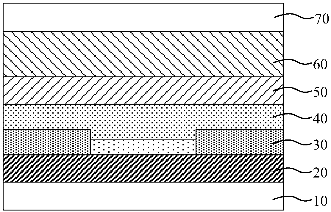
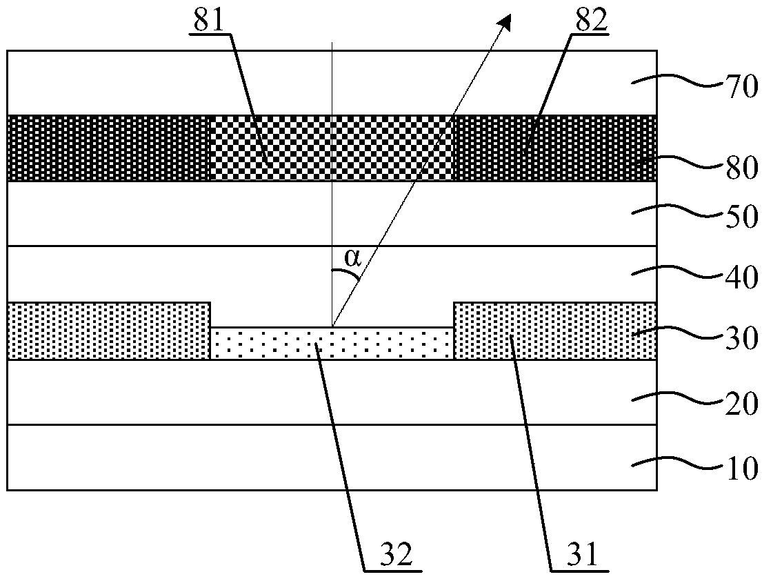
[0043] Image 6 It is a schematic structural diagram of an OLED panel according to the first embodiment of the present invention. from Image 6 It can be seen from the figure that the OLED panel of this embodiment includes a substrate 10 , a TFT array layer 20 , an organic light emitting layer 30 and a color filter layer 80 . Wherein, the TFT array layer 20 is disposed on the substrate 10 , and the organic light emitting layer 30 is disposed on the TFT array layer 20 . The organic light emitting layer 30 includes an OLED pixel 32 and a pixel defining layer 31 defining an area of ​​the OLED pixel 32 . The color filter layer 80 is disposed on the organic light emitting layer 30 , and the color filter layer 80 includes a color filter 81 disposed on the OLED pixels 32 , and the color filter 81 is arranged in a one-to-one correspondence with the OLED pixels 32 .

[0044] The color filter 81 is disposed on the OLED pixel 32 , so that the light emitted by the OLED pixel 32 is emit...

no. 2 example

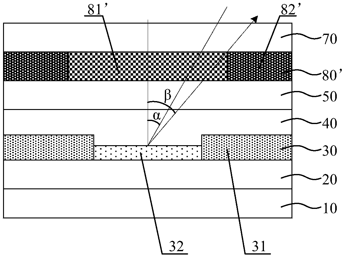
[0054] Figure 7 It is a schematic structural diagram of an OLED panel according to the second embodiment of the present invention. Different from the first embodiment, in this embodiment, if Figure 7 As shown, the OLED panel further includes a protective film layer 90 located between the organic light emitting layer 30 and the color filter layer 80 . The protective film layer 90 can further protect the OLED pixel 32 and the cathode of the OLED pixel 32, and further improve the water and oxygen barrier performance of the OLED panel.

[0055] The material of the protective film layer 90 includes at least one of silicon nitride and silicon oxide. In a specific implementation, the material of the protective film layer 90 may be silicon nitride, silicon oxide or a mixture of silicon nitride and silicon oxide. After the organic light emitting layer 30 is formed, the protective film layer 90 may be formed on the organic light emitting layer 30 by evaporation. The thickness of t...

no. 3 example

[0057] Figure 8 It is a schematic structural diagram of an OLED panel according to a third embodiment of the present invention. from Figure 8 It can be seen from the figure that the OLED panel of this embodiment includes a substrate 10 , a TFT array layer 20 , an organic light emitting layer 30 and a color filter layer 80 . Wherein, the TFT array layer 20 is disposed on the substrate 10 , and the organic light emitting layer 30 is disposed on the TFT array layer 20 . The organic light emitting layer 30 includes an OLED pixel 32 and a pixel defining layer 31 defining an area of ​​the OLED pixel 32 . The color filter layer 80 is disposed on the organic light emitting layer 30 . Different from the first embodiment, in this embodiment, the color filter layer 80 includes a color filter 81 disposed on the OLED pixel 32 .

[0058] In addition, in this embodiment, the material of the pixel defining layer 31 is a black opaque material, such as black resin material, etc., so that ...


PUM


Abstract

The invention discloses an OLED panel and a display device. The OLED panel includes a substrate, an organic light emitting layer disposed on the substrate, and a color filter layer disposed on the organic light emitting layer. The organic light emitting layer includes an OLED pixel, and the color filter layer includes a color film disposed on the OLED pixel. The OLED panel, the distance between the color film and the OLED pixel is greatly reduced compared with the prior art, The large viewing angle brightness attenuation angle of the OLED panel is increased, so that the large viewing angle brightness attenuation angle can be increased without increasing the color film aperture ratio, and the large viewing angle brightness attenuation angle is increased while maintaining the low reflectivity of the OLED panel, which is favorable for realizing the outdoor visualization function and the lightness of the OLED panel.

Description

technical field [0001] The invention relates to the field of display technology, in particular to an OLED panel and a display device. Background technique [0002] In the prior art, in order to realize the outdoor visual function of the organic light emitting diode (Organic Light Emitting Diode, OLED) panel, the display side of the OLED panel is provided with a linear polarizing layer (POL) to reduce the reflection of external ambient light and realize Outdoor viewing capabilities of OLED panels. Generally, the light transmittance of POL is 44%, the reflectance is 5%, and its thickness is greater than 50 μm. Such a thickness of POL is not conducive to realizing flexible display characteristics such as folding and curling of OLED panels. In order to realize flexible display characteristics, it is necessary to reduce the thickness of POL. At present, color film is usually used instead of POL to facilitate the realization of light and thin OLED panels. [0003] However, aft...

Claims


Application Information

Patent Timeline
Patent Type & Authority Applications(China)
IPC IPC(8): H01L27/32
CPCH10K59/50
Inventor 祝文秀史世明
Owner BOE TECH GRP CO LTD
Why Eureka
Try Eureka