A Slow Wave Structure of Plane Slots

A technology of slow-wave structure and planar slot line, which is applied to the circuit components of time-of-flight electron tubes, etc., can solve the problems that electric vacuum devices cannot reach 100%, affect the performance of slow-wave structures, and travelling-wave tubes cannot work. Achieve the effects of flat coupling impedance curve, low operating voltage, and small gain fluctuation

Inactive Publication Date: 2017-12-19
UNIV OF ELECTRONICS SCI & TECH OF CHINA
View PDF6 Cites 0 Cited by
  • Summary
  • Abstract
  • Description
  • Claims
  • Application Information

AI Technical Summary

Problems solved by technology

However, there are some key problems in this kind of planar slow wave structure that restrict the development of miniaturized traveling wave tubes based on this kind of slow wave structure. One of them is the problem of electron accumulation on the dielectric substrate. It is impossible to achieve 100% in practice, that is to say, when vacuum devices are working, there will always be electrons hitting the slow wave structure. Traditional devices such as helical traveling wave tubes are bulky and heavy, but because electrons generally It is directly hit on the metal helix with good electrical conductivity, so electrons can be directly guided away
However, the current planar slow wave structures are all processed on the dielectric substrate by means of printed circuit boards. It will accumulate on the dielectric substrate, causing the potential to drop, thereby changing the focus of the electron beam. This process will not only destroy the dielectric substrate, affect the performance of the slow wave structure, but also cause the traveling wave tube to fail to work in severe cases.

Method used


Image

  • A Slow Wave Structure of Plane Slots
  • A Slow Wave Structure of Plane Slots
  • A Slow Wave Structure of Plane Slots

Examples


Embodiment

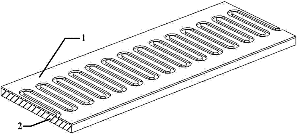
[0025] A coplanar waveguide slow-wave structure, such as figure 1 The shown N-shaped groove line slow wave structure, which is a schematic structural diagram of a specific embodiment of the present invention, includes a dielectric substrate 2 and a metal layer 1 located on the surface of the dielectric substrate 2, and a groove line is engraved on the metal layer 1 , the shape of the groove line is a periodic bending curve.

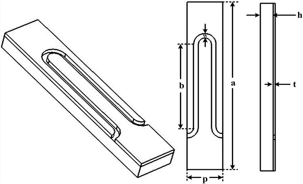
[0026] like figure 2 As shown, the dimensions defining the above slot line slow wave structure are as follows: the dielectric constant of the dielectric substrate 2 is ε, the thickness of the dielectric substrate is h, the transverse length is a, the period length is p, the slot line width is w, and the microstrip thickness is t, the length of the straight part of the groove line is b. The dimensions of the structure of the specific embodiment are as follows (unit: mm): a=1.4, b=0.5, p=0.28, w=0.05, t=0.05, h=0.4.

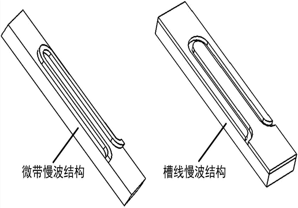
[0027] like image 3 As shown, in ...


PUM


Abstract

The invention discloses a slow wave structure of plane slot lines, belongs to the field of microwave electric vacuum technology, and relates to a traveling wave tube amplifier. The invention comprises a dielectric substrate (2) and a metal layer (1) located on the surface of the dielectric substrate (2). A groove line is engraved on the metal layer (1), and the shape of the groove line is a periodic bending curve. The present invention can prevent the unconstrained electrons from directly hitting the dielectric substrate due to disturbance, thereby effectively solving the problem of electron accumulation in the microstrip slow-wave structure; the vacuum device adopting the structure of the present invention has a lower operating voltage and its dispersion curve Relatively flat, so that the electron injection can be synchronized with the electromagnetic wave in a wider frequency band, and then realize the broadband design of the vacuum device; the coupling impedance curve of the vacuum device adopting the structure of the present invention is very flat, indicating that its gain fluctuation in the working frequency band Compared with the microstrip slow-wave structure, it is smaller. Therefore, the invention has great potential and market value in the slow wave structure of the miniaturized planar traveling wave tube.

Description

technical field [0001] The design of the invention belongs to the field of microwave electric vacuum technology, and relates to a traveling wave tube amplifier. Background technique [0002] As an important microwave and millimeter wave source, electric vacuum devices are widely used in radar, guidance, communication, microwave remote sensing and other fields. They are known as the "heart" of weapons and equipment, and their performance directly determines the level of the overall equipment. With the rapid development of aerospace engineering and electronic technology, there is an urgent need for power sources with relatively simple structure and processing technology, broadband, high power, small volume, and low cost. How to achieve miniaturization and low voltage while ensuring the advantages of high power, high efficiency, high frequency band, and wide bandwidth of electric vacuum devices, so as to better meet the needs of technological development, is an important develo...

Claims


Application Information

Patent Timeline
Patent Type & Authority Patents(China)
IPC IPC(8): H01J23/28
CPCH01J23/28H01J2223/30
Inventor 丁冲魏彦玉王媛媛张鲁奇李倩郭彍宫玉彬王文祥
Owner UNIV OF ELECTRONICS SCI & TECH OF CHINA
Why Eureka
Try Eureka