Light responsive semiconductor switch with shorted load protection

a technology of shorted load protection and semiconductor switch, which is applied in the direction of semiconductor/solid-state device details, pulse technique, radiation control devices, etc., can solve the problems of not being able to protect the load circuit as well as the output switching transistor, and it is difficult to combine the two requirements against the use of photovoltaic elements of varying current generation capacity

Inactive Publication Date: 2002-01-15
MATSUSHITA ELECTRIC WORKS LTD
View PDF7 Cites 65 Cited by
  • Summary
  • Abstract
  • Description
  • Claims
  • Application Information

AI Technical Summary

Benefits of technology

The characterizing feature of the present invention resides in that the shunt transistor and the current limiting resistive element are formed separately from the latch circuit, and that the current limiting resistive element is connected between the control electrode of the output switching transistor and the positive electrode of the photovoltaic element so as to limit the current from the photovoltaic element, when said shunt transistor is conductive, to such an extent as to lower the operating voltage being applied to the control electrode of the output switching transistor below the threshold voltage, while allowing the photovoltaic element to provide a supply voltage to the latch circuit for holding the interruption signal. Thus, the series combination of the current limiting resistive element and the shunt transistor which are separately formed from the latch circuit can assure to provide the supply voltage to the latch circuit and at the same time to limit the operative voltage being applied to the control electrode of the output switching transistor, so as to keep the interruption signal from the latch circuit on one hand, and to turn off the output switching transistor without fail in response to the interruption signal on the other hand, enabling successful and reliable interruption of the overcurrent. Also, since the current limiting resistive element is separately formed from the latch circuit, it is readily possible to assure the above interruption of the overcurrent irrespective of varying current generating capacity of the photovoltaic element, simply by selecting the impedance of the current limiting resistive element. With this result, the output transistor can be protected completely from the overcurrent in the load circuit.
Moreover, the switch may include a delay timer which delays providing the overcurrent signal from the overcurrent sensor to the latch circuit for a short time period immediately upon the photovoltaic element generating the electric power, thereby canceling a transient voltage appearing across the current sensing resistor immediately after the activation of the photovoltaic element. With the inclusion of the delay timer, the output switching transistor can be prevented from responding to noncritical overcurrent appearing immediately after the actuation of the photovoltaic element for assuring reliable switching operation.

Problems solved by technology

With this restriction to the shunt transistor common to the latch circuit, it is rather difficult to combine the two requirements against the use of the photovoltaic element of varying current generating capacity.
For example, when the photovoltaic element having a large current generating capacity is used to apply a correspondingly high voltage to the control electrode of the output transistor for rapidly turning it on, the conduction of the shunt transistor made for the latching operation may not be enough to lower the voltage applied to the control electrode of the output transistor below a threshold voltage thereof, failing to turn off the output transistor even when the shunt transistor is made conductive to draw the current from the photovoltaic element.
Accordingly, the prior switch poses limitations to a circuit design and is not satisfactory for complete interruption of the overcurrent irrespective of the current generating capacity of the photovoltaic element.
If this should occur, the latch circuit would be reset to turn off the shunt transistor, disabling the interruption of the overcurrent in the load circuit, failing to protect the load circuit as well as the output switching transistor.
Moreover, the switch may include a delay timer which delays providing the overcurrent signal from the overcurrent sensor to the latch circuit for a short time period immediately upon the photovoltaic element generating the electric power, thereby canceling a transient voltage appearing across the current sensing resistor immediately after the activation of the photovoltaic element.

Method used


Image

  • Light responsive semiconductor switch with shorted load protection
  • Light responsive semiconductor switch with shorted load protection
  • Light responsive semiconductor switch with shorted load protection

Examples


first embodiment

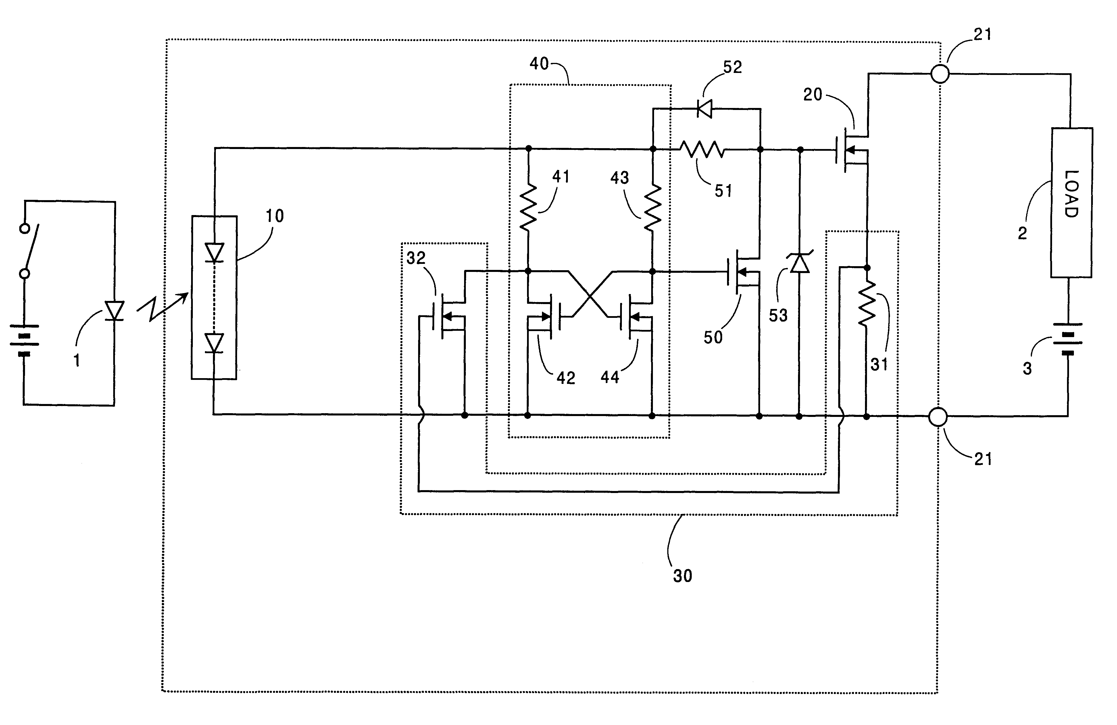
Referring now to FIG. 1, there is shown a light responsive semiconductor switch in accordance with a first embodiment of the present invention. The switch is utilized in combination with a light emitting diode 1 to constitute an optical relay for connecting and disconnecting a load 2 to and from its power source 3. The switch includes a photovoltaic element 10 in the form of a photo-diode array which generates an electric power upon absorption of a light from the light emitting diode 1. The electric power gives an operating voltage which decreases with an increasing current from the photo-diode array 10. The operating voltage is applied to trigger an output switching transistor 20 in the form of an n-channel enhancement metal oxide field-effect transistor (MOSFET) whose gate-source is connected across the photo-diode array 10. The output MOSFET 20 has a drain and a source connected respectively to output terminals 21 which are adapted in use for connection with a load circuit compos...

second embodiment

Referring to FIG. 4, there is shown a light responsive semiconductor switch in accordance with a second embodiment of the present invention. The switch of this embodiment is designed for a load circuit of energizing the load 2 with an AC power source 3A, and is identical to the first embodiment except for the use of an additional output MOSFET 22 and for the inclusion of an additional current sensing resistor 33, and an additional sensor MOSFET 34 in the overcurrent sensor 30A. Like elements are designated by like reference numerals with a suffix letter of "A". The additional output MOSFET 22 is connected in series with the output MOSFET 20A between the output terminals 21A with the sources of MOSFETs 20A and 22 being connected to each other and with the gates of MOSFETs 20A and 22 being commonly connected to receive the operating voltage from the photo-diode array 10A. The additional resistor 33 is connected in series with resistor 31A between the output terminals 21A to provide a ...

third embodiment

Referring to FIG. 7, there is shown a light responsive semiconductor switch in accordance with a third embodiment of the present invention which is identical to the first embodiment except for the inclusion of a bypass MOSFET 35 in the overcurrent sensor 30D. Like elements are designated by like reference numerals with a suffix letter of "D". The bypass MOSFET 35 has its source-drain connected in series with the current sensing resistor 31D across the drain-source of the output MOSFET 20D, and has its gate to the gate of the output MOSFET 20D to commonly receive the operating voltage from the photo-diode array 10D. The bypass MOSFET 35 and the resistor 31D form a high resistance path across the output MOSFET 20D to flow a fraction of the load current through the resistor 31D merely for detection of the overcurrent, allowing to flow the substantial load current through the output MOSFET 20D. When the overcurrent sensor 30D detects the overcurrent, the latch circuit 40D responds to ke...


PUM


Abstract

An improved light responsive semiconductor switch with shorted load protection capable of successfully interrupting a load overcurrent. The switch is includes an output transistor which is triggered by a photovoltaic element to connect a load to a power source thereof, and an overcurrent sensor which provides an overcurrent signal upon seeing an overcurrent condition in the load. A shunt transistor is connected in series with a current limiting resistive element across the photovoltaic element to define a shunt path of flowing the current from the photovoltaic element through the current limiting resistive element away from the output transistor. A latch circuit is included to be energized by the photovoltaic element and to provide an interruption signal once the overcurrent signal is received and hold the interruption signal. The interruption signal turns on the shunt transistor so as to flow the current from the photovoltaic element through the shunt path, thereby turning off the output transistor for interruption of the overcurrent. The current limiting resistive element is connected in series with the shunt transistor to limit the current from the photovoltaic element when the shunt transistor is turned on, thereby providing a supply voltage from the photovoltaic element to the latch circuit. Thus, the latch circuit is enabled to keep providing the interruption signal for reliable interruption of the overcurrent.

Description

1. Field of the InventionThe present invention relates to a light responsive semiconductor switch with shorted load protection for use in an optical relay.2. Description of the Prior ArtJapanese Patent Publication No. 11-163706 discloses a light responsive semiconductor switch for use in an optical relay. The switch includes a photovoltaic element which provides an operating voltage upon absorption of light from a light source, and an output transistor which is triggered by the operating voltage to become conductive for connecting a load to a power source. In order to protect the output transistor from an overcurrent due to an accidental short-circuiting of the load, the switch includes an overcurrent sensor for detection of the overcurrent condition, and a shunt transistor which, in response to the overcurrent condition, becomes conductive to flow the current from the photovoltaic element away from the output transistor to turn if off for interruption of the overcurrent. Further, t...

Claims


Application Information

Patent Timeline
Patent Type & Authority Patents(United States)
IPC IPC(8): H03K17/785H03K17/082H03K3/00H03K3/356H03K17/78
CPCH03K17/785H03K17/0822H03K3/356
Inventor TOMII, KAZUSHINAGAHAMA, HIDEOHAGIHARA, YOSUKE
Owner MATSUSHITA ELECTRIC WORKS LTD
Why Eureka
Try Eureka